


目录
一、未使用的PIN设置
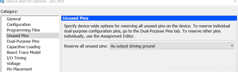
1. 当所有的未使用的PIN设置为输出接地时:
主要指:所有的IC PIN,包括已经定义了输入或者输出的PIN,但是没有实际的信号进出(即未使用),测试为0v。
反面讲,使用的PIN,是指实际定义并在逻辑里使用这个信号,且有实际负载的才算。否则就算定义了,如果没有实际使用也是未使用。
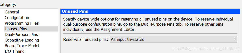
2. 当所有的未使用的PIN设置为三态输入:
3.设置为若上拉或者三态时
如果在PIN PLANNER中定义了输入弱上拉,那么未使用时测试为高电平。其余PIN受set the unused pins as "inputs tri-stated with weak pull up",控制,为低电平。
测得的高电平电压与I/O bank standard设置电压的关系如下:
外部硬件将Bank接到3.3v,
1) 对于输入PIN,无负载时来说:如果设置了若上拉,那么I/O bank 电压为3.3v,2.5v或者1.8v时均测得 2.0v;如果没有若上拉,那么均测得0v;
2) 对于输出PIN,若上拉没有关系;I/O bank设置为3.3v, 2.5v,1.8v时测得输出高电平电压为均为3.3V;
3)如果是没有定义的pin,测得的电压为外部bank的供电电压。
因此,I/O bank 电压标准只是用于FPGA判断输入或者输出的电平为高或者低,二实际PIN脚的电压只与硬件供电电压有关。
4. 一般情况下设置为三态输入或者三态弱上拉输入。同时硬件需要外部处理如下:
If you set the unused pins as "inputs tri-stated" in the Quartus® II software, you should connect the pins on the PCB to VCCIO, GND, or a static signal for better noise immunity.
If you set the unused pins as "inputs tri-stated with weak pull up", you do not have to connect the pin on the board. The internal pull up to VCCIO will bias the pin and prevent it from floating.
如果不设置,可能发生情况:
If your dedicated input or IO pins are left floating, then the input transistors might fall outside of the saturation or cut-off region. As a result, the device could draw additional current and increase the device's power consumption.
Additionally, if left floating, these pins are apt to switch (they behave similar to antennas) which can inject noise into the device.
As such, Altera recommends connecting these dedicated pins to the appropriate logic level defined by the Altera® software pin file (typically either VCC or GND).
二、I/Obank电压
FPGA逻辑电平只有3.3V,2.5V的,1.8V只用于差分信号使用。
如果硬件设置了bank电压为2.5v,那么作为输出时这个bank只能驱动2.5v的外设,作为输入可以接收2.5/3.3v的电压。
另外不同bank可以支持不同的i/o标准,但是同一bank的电压最好是同一标准。


 1310
1310

 被折叠的 条评论
为什么被折叠?
被折叠的 条评论
为什么被折叠?
 到【灌水乐园】发言


