


 本文围绕APB slave设计展开,介绍了基于APB协议完成寄存器配置或读取的设计实例,包括其数据总线、寄存器类型等规格。还对apb_slave_interface、apb_slave_reg等代码进行分析,给出顶层apb4_eg_slave设计代码的参考链接。
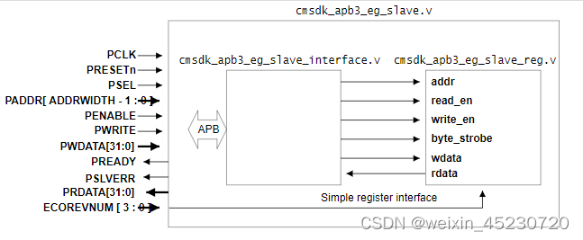
APB slave设计spec
参考ARM公司的例子得到的,链接如下,
APB3.0例子
APB4.0例子
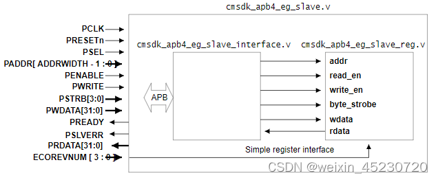
一个简单的APB从接口。
32位数据总线,端独立。对于APB3从机示例,数据处理仅为32位。对于APB4从机示例,使用PSTRB信号对单个字节执行写操作。
数据传输需要两个时钟周期。
4个32位RW寄存器
该模块是一个基于APB协议完成寄存器配置或读取的设计实例,上面APB相关的信号都介绍过,这里不再重复介绍,其中的ECOREVNUM的意思是ECO revision number,如果没有用到ARM的ECO的话,将该信号固定为全0即可。右边这个slave_reg实际上就对应我们自己设计的IP的寄存器配置部分。这一部分的接口是native interface,也就是没有考虑通用性的原生接口。想要通过APB总线对其进行配置,就需要通过slave_interface这个模块进行协议转换,进而完成APB协议的传输.
- 不支持反压
- 不支持错误传输
- 支持4个RW类型的寄存器
- 支持12个RO类型寄存器
- 支持字节选通信号
APB slave设计代码
apb_slave_interface代码
//------------------------------------------------------------------------------
// The confidential and proprietary information contained in this file may
// only be used by a person authorised under and to the extent permitted
// by a subsisting licensing agreement from ARM Limited.
//
//            (C) COPYRIGHT 2010-2015  ARM Limited or its affiliates.
//                ALL RIGHTS RESERVED
//
// This entire notice must be reproduced on all copies of this file
// and copies of this file may only be made by a person if such person is
// permitted to do so under the terms of a subsisting license agreement
// from ARM Limited.
//
//  Version and Release Control Information:
//
//  File Revision       : $Revision: 275084 $
//  File Date           : $Date: 2014-03-27 15:09:11 +0000 (Thu, 27 Mar 2014) $
//
//  Release Information : Cortex-M0 DesignStart-r1p0-00rel0
//------------------------------------------------------------------------------
// Verilog-2001 (IEEE Std 1364-2001)
//------------------------------------------------------------------------------
//
//-----------------------------------------------------------------------------
// Abstract : AMBA APB4 example slave interface module. Transfer APB BUS protocol to
//            simple register read write protocol
//-----------------------------------------------------------------------------
module cmsdk_apb4_eg_slave_interface #(
  // parameter for address width
  parameter ADDRWIDTH = 12)
 (
  // IO declaration

  input  wire                    pclk,     // pclk
  input  wire                    presetn,  // reset

  // apb interface inputs
  input  wire                    psel,
  input  wire [ADDRWIDTH-1:0]    paddr,
  input  wire                    penable,
  input  wire                    pwrite,
  input  wire [31:0]             pwdata,
  input  wire [3:0]              pstrb,

  // apb interface outputs
  output wire [31:0]             prdata,
  output wire                    pready,
  output wire                    pslverr,

  //Register interface
  output wire [ADDRWIDTH-1:0]    addr,
  output wire                    read_en,
  output wire                    write_en,
  output wire [3:0]              byte_strobe,
  output wire [31:0]             wdata,
  input  wire [31:0]             rdata);


 //------------------------------------------------------------------------------
 // module logic start
 //------------------------------------------------------------------------------

// APB interface
assign   pready  = 1'b1; //always ready. Can be customized to support waitstate if required.
assign   pslverr = 1'b0; //always OKAY. Can be customized to support error response if required.


// register read and write signal
assign  addr = paddr;
assign  read_en  = psel & (~pwrite); // assert for whole apb read transfer
assign  write_en = psel & (~penable) & pwrite; // assert for 1st cycle of write transfer
        // It is also possible to change the design to perform the write in the 2nd
        // APB cycle.   E.g.
        //   assign write_en = psel & penable & pwrite;
        // However, if the design generate waitstate, this expression will result
        // in write_en being asserted for multiple cycles.
assign  byte_strobe = pstrb;
assign  wdata       = pwdata;
assign  prdata      = rdata;

`ifdef ARM_APB_ASSERT_ON

 `include "std_ovl_defines.h"
  // ------------------------------------------------------------
  // Assertions
  // ------------------------------------------------------------

  // Check error response should not be generated if not selected
    assert_never
     #(`OVL_ERROR,
       `OVL_ASSERT,
       "Error! Should not generate error response if not selected")
     u_ovl_apb4_eg_slave_response_illegal
     (.clk        (pclk),
      .reset_n    (presetn),
      .test_expr  (pslverr & pready & (~psel))
      );

`endif
 //------------------------------------------------------------------------------
 // module logic end
 //------------------------------------------------------------------------------

endmodule
我们对其进行分析:
- 首先由于不支持反压和错误传输,因此将pready固定为1,pslverr固定为0。
- APB传输进来的paddr可以直接赋给addr,作为读写的地址。
- read_en需要在psel为1且pwrite为0的时候拉高。这实际上是希望在整个读传输过程中都让read_en信号有效。读者可能就想问了,读应该对应着两个阶段吗?不需要判断吗?实际上读的话,master那边自己控制好就行了,对于slave而言完全可以在第一拍和第二拍都把rdata提供好,这个是没有关系的
- write_en则对应着setup phase,实际上在这个场景中修改write_en的逻辑让该信号对应着access phase也是可以的
- 其它的信号直接赋值就可以,应该很好理解.
apb_slave_reg代码
//------------------------------------------------------------------------------
// The confidential and proprietary information contained in this file may
// only be used by a person authorised under and to the extent permitted
// by a subsisting licensing agreement from ARM Limited.
//
//            (C) COPYRIGHT 2010-2015  ARM Limited or its affiliates.
//                ALL RIGHTS RESERVED
//
// This entire notice must be reproduced on all copies of this file
// and copies of this file may only be made by a person if such person is
// permitted to do so under the terms of a subsisting license agreement
// from ARM Limited.
//
//  Version and Release Control Information:
//
//  File Revision       : $Revision: 275084 $
//  File Date           : $Date: 2014-03-27 15:09:11 +0000 (Thu, 27 Mar 2014) $
//
//  Release Information : Cortex-M0 DesignStart-r1p0-00rel0
//------------------------------------------------------------------------------
// Verilog-2001 (IEEE Std 1364-2001)
//------------------------------------------------------------------------------
//
//-----------------------------------------------------------------------------
// Abstract : APB example slave register module.
//            Support AMBA APB4
//            This is an example slave with four 32-bit registers, provides write
//            and read operation. The Data and address valid at the same clock
//            cycle. Byte strobe signal is supported.
//-----------------------------------------------------------------------------

module cmsdk_apb4_eg_slave_reg #(
  // parameter for address width
  parameter   ADDRWIDTH = 12)
 (
  input  wire                   pclk,       // clock
  input  wire                   presetn,    // reset

  // Register interface
  input  wire [ADDRWIDTH-1:0]   addr,
  input  wire                   read_en,
  input  wire                   write_en,
  input  wire [3:0]             byte_strobe,
  input  wire [31:0]            wdata,
  input  wire [3:0]             ecorevnum,
  output reg  [31:0]            rdata);

  // Local ID parameters, APB4 example slave has part number of 819
localparam  ARM_CMSDK_APB4_EG_SLAVE_PID4 = 32'h00000004; // 0xFD0 : PID 4
localparam  ARM_CMSDK_APB4_EG_SLAVE_PID5 = 32'h00000000; // 0xFD4 : PID 5
localparam  ARM_CMSDK_APB4_EG_SLAVE_PID6 = 32'h00000000; // 0xFD8 : PID 6
localparam  ARM_CMSDK_APB4_EG_SLAVE_PID7 = 32'h00000000; // 0xFDC : PID 7
localparam  ARM_CMSDK_APB4_EG_SLAVE_PID0 = 32'h00000019; // 0xFE0 : PID 0 APB4 Example slave part number[7:0]
localparam  ARM_CMSDK_APB4_EG_SLAVE_PID1 = 32'h000000B8; // 0xFE4 : PID 1 [7:4] jep106_id_3_0. [3:0] part number [11:8]
localparam  ARM_CMSDK_APB4_EG_SLAVE_PID2 = 32'h0000001B; // 0xFE8 : PID 2 [7:4] revision, [3] jedec_used. [2:0] jep106_id_6_4
localparam  ARM_CMSDK_APB4_EG_SLAVE_PID3 = 32'h00000000; // 0xFEC : PID 3
localparam  ARM_CMSDK_APB4_EG_SLAVE_CID0 = 32'h0000000D; // 0xFF0 : CID 0
localparam  ARM_CMSDK_APB4_EG_SLAVE_CID1 = 32'h000000F0; // 0xFF4 : CID 1 PrimeCell class
localparam  ARM_CMSDK_APB4_EG_SLAVE_CID2 = 32'h00000005; // 0xFF8 : CID 2
localparam  ARM_CMSDK_APB4_EG_SLAVE_CID3 = 32'h000000B1; // 0xFFC : CID 3
         // Note : Customer changing the design should modify
         // - jep106 value (www.jedec.org)
         // - part number (customer define)
         // - Optional revision and modification number (e.g. rXpY)


 //------------------------------------------------------------------------------
 // internal signals
 //------------------------------------------------------------------------------

  reg    [31:0]            data0;
  reg    [31:0]            data1;
  reg    [31:0]            data2;
  reg    [31:0]            data3;
  wire   [3:0]             wr_sel;

 //------------------------------------------------------------------------------
 // module logic start
 //------------------------------------------------------------------------------
  // Address decoding for write operations
  assign wr_sel[0] = ((addr[(ADDRWIDTH-1):2]==10'b0000000000)&(write_en)) ? 1'b1: 1'b0;
  assign wr_sel[1] = ((addr[(ADDRWIDTH-1):2]==10'b0000000001)&(write_en)) ? 1'b1: 1'b0;
  assign wr_sel[2] = ((addr[(ADDRWIDTH-1):2]==10'b0000000010)&(write_en)) ? 1'b1: 1'b0;
  assign wr_sel[3] = ((addr[(ADDRWIDTH-1):2]==10'b0000000011)&(write_en)) ? 1'b1: 1'b0;


 // register write, byte enable


 // Data register: data0
  always @(posedge pclk or negedge presetn)
    begin
    if (~presetn)
      begin
        data0 <= {32{1'b0}}; // Reset data 0 to 0x00000000
      end
    else if (wr_sel[0])
      begin
        if (byte_strobe[0])
           data0[ 7: 0] <= wdata[ 7: 0];
        if (byte_strobe[1])
           data0[15: 8] <= wdata[15: 8];
        if (byte_strobe[2])
           data0[23:16] <= wdata[23:16];
        if (byte_strobe[3])
           data0[31:24] <= wdata[31:24];
      end
    end


 // Data register: data1
  always @(posedge pclk or negedge presetn)
    begin
    if (~presetn)
      begin
        data1 <= {32{1'b0}}; // Reset data 1 to 0x00000000
      end
    else if (wr_sel[1])
      begin
        if (byte_strobe[0])
           data1[ 7: 0] <= wdata[7:0];
        if (byte_strobe[1])
           data1[15: 8] <= wdata[15:8];
        if (byte_strobe[2])
           data1[23:16] <= wdata[23:16];
        if (byte_strobe[3])
           data1[31:24] <= wdata[31:24];
      end
    end


  // Data register: data2
  always @(posedge pclk or negedge presetn)
    begin
    if (~presetn)
      begin
        data2 <= {32{1'b0}}; // Reset data 2 to 0x00000000
      end
    else if (wr_sel[2])
      begin
        if (byte_strobe[0])
           data2[ 7: 0] <= wdata[ 7: 0];
        if (byte_strobe[1])
           data2[15: 8] <= wdata[15: 8];
        if (byte_strobe[2])
           data2[23:16] <= wdata[23:16];
        if (byte_strobe[3])
           data2[31:24] <= wdata[31:24];
      end
    end


  // Data register: data3
  always @(posedge pclk or negedge presetn)
    begin
    if (~presetn)
      begin
        data3 <= {32{1'b0}}; // Reset data 3 to 0x00000000
      end
    else if (wr_sel[3])
      begin
        if (byte_strobe[0])
           data3[ 7: 0] <= wdata[ 7: 0];
        if (byte_strobe[1])
           data3[15: 8] <= wdata[15: 8];
        if (byte_strobe[2])
           data3[23:16] <= wdata[23:16];
        if (byte_strobe[3])
           data3[31:24] <= wdata[31:24];
      end
    end


 // register read

always @ (read_en or addr or data0 or data1 or data2 or data3 or ecorevnum)
 begin
   case (read_en)
     1'b1:
     begin
       if (addr[11:4] == 8'h00) begin
         case(addr[3:2])
           2'b00: rdata =  data0;
           2'b01: rdata =  data1;
           2'b10: rdata =  data2;
           2'b11: rdata =  data3;
           default: rdata = {32{1'bx}};
         endcase
       end
       else if (addr[11:6] == 6'h3F) begin
         case(addr[5:2])
          // Peripheral IDs and Component IDs.
          // AHB example slave has part number of 818
         4'b0100: rdata = ARM_CMSDK_APB4_EG_SLAVE_PID4; // 0xFD0 : PID 4
         4'b0101: rdata = ARM_CMSDK_APB4_EG_SLAVE_PID5; // 0xFD4 : PID 5
         4'b0110: rdata = ARM_CMSDK_APB4_EG_SLAVE_PID6; // 0xFD8 : PID 6
         4'b0111: rdata = ARM_CMSDK_APB4_EG_SLAVE_PID7; // 0xFDC : PID 7
         4'b1000: rdata = ARM_CMSDK_APB4_EG_SLAVE_PID0; // 0xFE0 : PID 0 APB Example slave part number[7:0]
         4'b1001: rdata = ARM_CMSDK_APB4_EG_SLAVE_PID1; // 0xFE4 : PID 1 [7:4] jep106_id_3_0. [3:0] part number [11:8]
         4'b1010: rdata = ARM_CMSDK_APB4_EG_SLAVE_PID2; // 0xFE8 : PID 2 [7:4] revision, [3] jedec_used. [2:0] jep106_id_6_4
         4'b1011: rdata ={ARM_CMSDK_APB4_EG_SLAVE_PID3[31:8], ecorevnum[3:0], 4'h0};
                                         // 0xFEC : PID 3 [7:4] ECO rev number, [3:0] modification number
         4'b1100: rdata = ARM_CMSDK_APB4_EG_SLAVE_CID0; // 0xFF0 : CID 0
         4'b1101: rdata = ARM_CMSDK_APB4_EG_SLAVE_CID1; // 0xFF4 : CID 1 PrimeCell class
         4'b1110: rdata = ARM_CMSDK_APB4_EG_SLAVE_CID2; // 0xFF8 : CID 2
         4'b1111: rdata = ARM_CMSDK_APB4_EG_SLAVE_CID3; // 0xFFC : CID 3
         // Note : Customer changing the design should modify
         // - jep106 value (www.jedec.org)
         // - part number (customer define)
         // - Optional revision and modification number (e.g. rXpY)
         4'b0000, 4'b0001,4'b0010,4'b0011: rdata = {32'h00000000}; // default
         default: rdata =  {32{1'bx}};  // x propagation
         endcase
       end
       else begin
         rdata = {32'h00000000}; // default
       end
   end
   1'b0:
     begin
       rdata =  {32{1'b0}};
     end
   default:
     begin
       rdata =  {32{1'bx}};
     end
   endcase
 end


 //------------------------------------------------------------------------------
 // module logic end
 //------------------------------------------------------------------------------


 endmodule
我们对其进行分析:
- 首先由于分为RW寄存器和RO寄存器。这里确定写地址是否在规定区间,同时写使能是否有效,以及byte_strobe信号,来决定要不要写,写哪个字节。
- 读的话就比较简单了,当读使能有效,根据地址信号决定rdata。实际上这就是个MUX选择逻辑。根据read_en加地址从多个寄存器的Q端选出某一个来。
顶层apb4_eg_slave设计代码
//------------------------------------------------------------------------------
// The confidential and proprietary information contained in this file may
// only be used by a person authorised under and to the extent permitted
// by a subsisting licensing agreement from ARM Limited.
//
//            (C) COPYRIGHT 2010-2015  ARM Limited or its affiliates.
//                ALL RIGHTS RESERVED
//
// This entire notice must be reproduced on all copies of this file
// and copies of this file may only be made by a person if such person is
// permitted to do so under the terms of a subsisting license agreement
// from ARM Limited.
//
//  Version and Release Control Information:
//
//  File Revision       : $Revision: 275084 $
//  File Date           : $Date: 2014-03-27 15:09:11 +0000 (Thu, 27 Mar 2014) $
//
//  Release Information : Cortex-M0 DesignStart-r1p0-00rel0
//------------------------------------------------------------------------------
// Verilog-2001 (IEEE Std 1364-2001)
//------------------------------------------------------------------------------
//
//-----------------------------------------------------------------------------
// Abstract : APB example slave, support AMBA APB4.
//            slave is always ready and response is always OKAY.
//-----------------------------------------------------------------------------

module  cmsdk_apb4_eg_slave #(
  // parameter for address width
  parameter ADDRWIDTH = 12)
 (
  // IO declaration
  input  wire                    PCLK,     // pclk
  input  wire                    PRESETn,  // reset

  // apb interface inputs
  input  wire                    PSEL,
  input  wire [ADDRWIDTH-1:0]    PADDR,
  input  wire                    PENABLE,
  input  wire                    PWRITE,
  input  wire [31:0]             PWDATA,
  input  wire [3:0]              PSTRB,

  input  wire [3:0]              ECOREVNUM, // Engineering-change-order revision bits

  // apb interface outputs
  output wire [31:0]             PRDATA,
  output wire                    PREADY,
  output wire                    PSLVERR);

//------------------------------------------------------------------------------
// internal wires
//------------------------------------------------------------------------------
  // Register module interface signals
  wire  [ADDRWIDTH-1:0]    reg_addr;
  wire                     reg_read_en;
  wire                     reg_write_en;
  wire  [3:0]              reg_byte_strobe;
  wire  [31:0]             reg_wdata;
  wire  [31:0]             reg_rdata;


//------------------------------------------------------------------------------
// module logic start
//------------------------------------------------------------------------------
 // Interface to convert APB signals to simple read and write controls
 cmsdk_apb4_eg_slave_interface
   #(.ADDRWIDTH (ADDRWIDTH))
   u_apb_eg_slave_interface(

  .pclk            (PCLK),     // pclk
  .presetn         (PRESETn),  // reset

  .psel            (PSEL),     // apb interface inputs
  .paddr           (PADDR),
  .penable         (PENABLE),
  .pwrite          (PWRITE),
  .pwdata          (PWDATA),
  .pstrb           (PSTRB),

  .prdata          (PRDATA),   // apb interface outputs
  .pready          (PREADY),
  .pslverr         (PSLVERR),

  // Register interface
  .addr            (reg_addr),
  .read_en         (reg_read_en),
  .write_en        (reg_write_en),
  .byte_strobe     (reg_byte_strobe),
  .wdata           (reg_wdata),
  .rdata           (reg_rdata)

  );

 // Example hardware register block
 cmsdk_apb4_eg_slave_reg
   #(.ADDRWIDTH (ADDRWIDTH))
   u_apb_eg_slave_reg (
  .pclk            (PCLK),
  .presetn         (PRESETn),

   // Register interface
  .addr            (reg_addr),
  .read_en         (reg_read_en),
  .write_en        (reg_write_en),
  .byte_strobe     (reg_byte_strobe),
  .wdata           (reg_wdata),
  .ecorevnum       (ECOREVNUM),
  .rdata           (reg_rdata)
  );

 //------------------------------------------------------------------------------
 // module logic end
 //------------------------------------------------------------------------------

`ifdef ARM_APB_ASSERT_ON

 `include "std_ovl_defines.h"
  // ------------------------------------------------------------
  // Assertions
  // ------------------------------------------------------------

   // Check the reg_write_en signal generated
    assert_implication
    #(`OVL_ERROR,
      `OVL_ASSERT,
      "Error! register write signal was not generated! "
      )
     u_ovl_apb4_eg_slave_reg_write
     (.clk             (PCLK),
      .reset_n         (PRESETn),
      .antecedent_expr ( (PSEL & (~PENABLE) & PWRITE) ),
      .consequent_expr ( reg_write_en == 1'b1)
      );


  // Check the reg_read_en signal generated
    assert_implication
    #(`OVL_ERROR,
      `OVL_ASSERT,
      "Error! register read signal was not generated! "
      )
     u_ovl_apb4_eg_slave_reg_read
     (.clk             (PCLK),
      .reset_n         (PRESETn),
      .antecedent_expr ( (PSEL & (~PENABLE) & (~PWRITE)) ),
      .consequent_expr ( reg_read_en == 1'b1)
      );


  // Check register read and write operation won't assert at the same cycle
    assert_never
     #(`OVL_ERROR,
       `OVL_ASSERT,
       "Error! register read and write active at the same cycle!")
     u_ovl_apb4_eg_slave_rd_wr_illegal
     (.clk         (PCLK),
      .reset_n     (PRESETn),
      .test_expr   ((reg_write_en & reg_read_en))
      );


`endif


endmodule
参考代码
参考文章


 271
271

 被折叠的 条评论
为什么被折叠?
被折叠的 条评论
为什么被折叠?
 到【灌水乐园】发言


