


 本文详细介绍了CMOS电路中的Schmitt触发器,它通过迟滞特性提供干净的脉冲输出。接着讨论了多谐振荡器的两种状态以及输入缓冲器的设计,特别是其在数字电路互联中的作用。此外,还涵盖了芯片上的电压发生器——电荷泵的工作原理。这些电路在噪声抑制和电源生成方面具有重要应用。
Chapter 18 Special Purpose CMOS Circuits
这一章讲几个实用电路, Schmitt trigger 输入信号noisy, 输出产生干净的pulse. 然后介绍multivibrator, 拥有astable和monostable两态. input buffer design 对于数字电路interconnecting 需要好的receiver. 最后介绍on-chip generator, 也就是charge pump.
The Schmitt Trigger
Schmitt Trigger本质就是一个带迟滞的比较器, 比较器在判断输入信号抖动时, 都应该加上迟滞
经典六管Schmitt Trigger
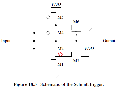
分析:
假设输入为Low, 输出=VDD, M1, M2 off, Vx=VDD- Vthn (接近4V).
当Vin < M1 threshold时, Vx 仍然为 VDD- Vthn
Trip Point: M2 开始 on, then Output开始下降, 导致M3开始off, 这会导致Vx下降更厉害
V
i
n
=
V
S
P
H
=
V
t
h
n
2
+
V
X
V_{in}=V_{SPH}=V_{thn2}+V_X
Vin=VSPH=Vthn2+VX
对于电流: M1和M3流过的电流一样, IM1=IM3
β
1
2
(
V
S
P
H
−
V
T
H
N
)
2
=
β
3
2
(
V
D
D
−
V
X
−
V
T
H
N
3
)
2
\frac{\beta_1}{2}(V_{SPH}-V_{THN})^{2}=\frac{\beta_3}{2}(VDD-V_{X}-V_{THN3})^{2}
2β1(VSPH−VTHN)2=2β3(VDD−VX−VTHN3)2
β 1 β 3 = W 1 L 3 L 1 W 3 = V D D − V S P H V S P H − V T H N \frac{\beta_1}{\beta_3}=\frac{W_1L_3}{L_1W_3}=\frac{VDD-V_{SPH}}{V_{SPH}-V_{THN}} β3β1=L1W3W1L3=VSPH−VTHNVDD−VSPH
上式可以计算Vin high switching point点
For M2 design rule, 因为M2用作Switch
β
2
>
β
1
or
β
3
\beta_2>\beta_1\text{ or }\beta_3
β2>β1 or β3
相似的考虑Vin lower switching point, trip point即M4 on, IM5=IM6
V
i
n
=
V
S
P
L
=
V
X
−
V
t
h
4
V_{in}=V_{SPL}=V_X-V_{th4}
Vin=VSPL=VX−Vth4
得到
β
5
β
6
=
W
5
L
6
L
5
W
6
=
V
S
P
L
V
D
D
−
V
S
P
L
−
V
T
H
P
\frac{\beta_5}{\beta_6}=\frac{W_5L_6}{L_5W_6}=\frac{V_{SPL}}{VDD-V_{SPL}-V_{THP}}
β6β5=L5W6W5L6=VDD−VSPL−VTHPVSPL
通过上述公式可求得M1M3 M5M6的宽长比
Switching Characteristic
propagation delay:
t
P
H
L
=
0.7
(
R
n
1
+
R
n
2
)
C
l
o
a
d
t_{PHL}=0.7(R_{n1}+R_{n2})C_{load}
tPHL=0.7(Rn1+Rn2)Cload
Application of Schmtt Trigger
1, 用于clean up an interconnect signal, 防止输出来回震荡
2, Oscillator
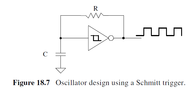
Cap电压作为Schmtt在Vsph和Vspl之间反复跳转, 经过RC充放电
RC放电: Vc从VSPH放电到VSPL
V
c
=
V
S
P
H
e
−
t
/
R
C
V_c=V_{SPH}e^{-t/RC}
Vc=VSPHe−t/RC
t 1 = R C ⋅ l n V S P H V S P L t_1=RC\cdot ln\frac{V_{SPH}}{V_{SPL}} t1=RC⋅lnVSPLVSPH
RC充电: Vc从VSPL充电到VSPH
V
c
=
V
S
P
L
+
(
V
D
D
−
V
S
P
L
)
(
1
−
e
−
t
/
R
C
)
V_c=V_{SPL}+(VDD-V_{SPL})(1-e^{-t/RC})
Vc=VSPL+(VDD−VSPL)(1−e−t/RC)
t 2 = R C ⋅ l n V D D − V S P L V D D − V S P H t_2=RC\cdot ln\frac{VDD-V_{SPL}}{VDD-V_{SPH}} t2=RC⋅lnVDD−VSPHVDD−VSPL
Oscillator频率
f
o
s
c
=
1
t
1
+
t
2
f_{osc}=\frac{1}{t_1+t_2}
fosc=t1+t21
另外一种Oscillator
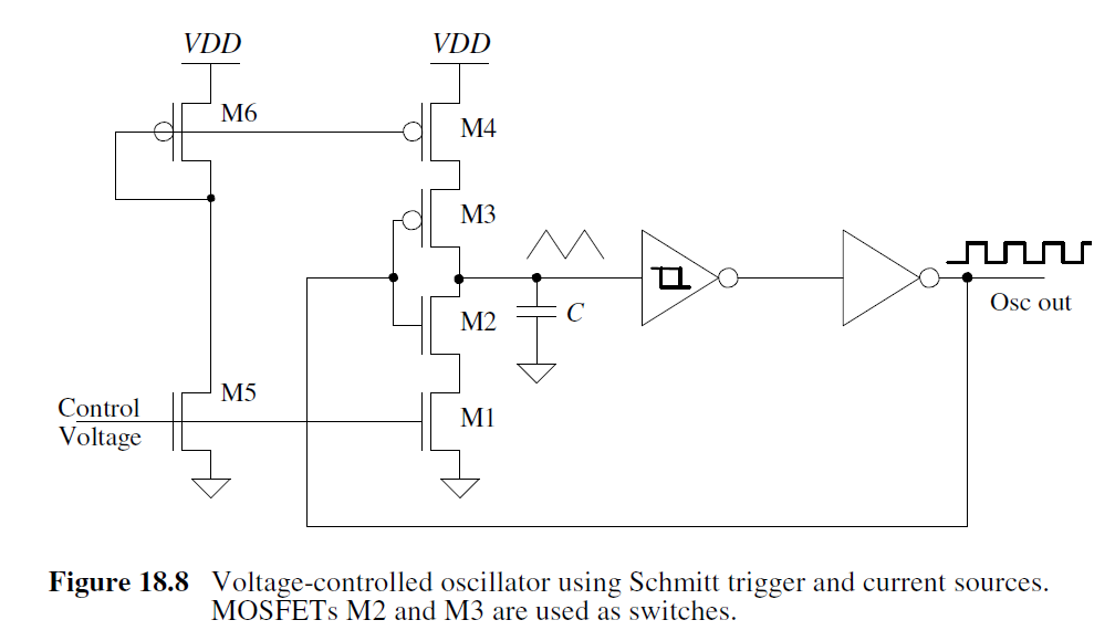
M2和M3作为Switch, M4电流ID4, M1电流ID1
电容从VSPL充到VSPH:
t
1
=
C
V
S
P
H
−
V
S
P
L
I
D
4
t_1=C\frac{V_{SPH}-V_{SPL}}{I_{D4}}
t1=CID4VSPH−VSPL
电容从VSPH放电到VSPL:
t
2
=
C
V
S
P
H
−
V
S
P
L
I
D
1
t_2=C\frac{V_{SPH}-V_{SPL}}{I_{D1}}
t2=CID1VSPH−VSPL
Oscillator频率
f
o
s
c
=
1
t
1
+
t
2
f_{osc}=\frac{1}{t_1+t_2}
fosc=t1+t21
Multivibrator Circuits
Multivibrator 也可以称为function generator
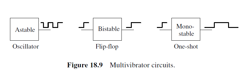
The monostable即 one-shot circuit
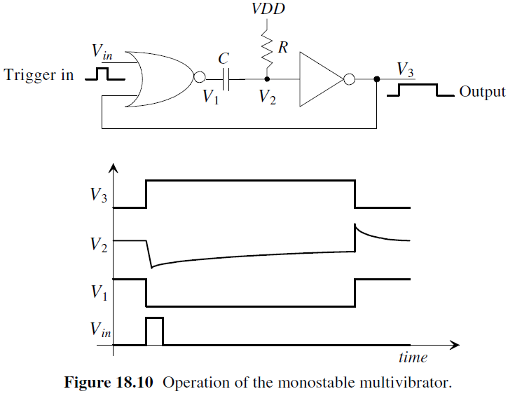
一开始Vin=0, V2=VDD, V3=0, V1 = VDD. 当Trigger信号来临, Vin翻高, V1 = 0, 把 V2拉下来=0, V3=VDD. V2被RC慢慢拉到VDD, V3最终在降为0
V
2
=
V
0
+
(
V
1
−
V
0
)
[
1
−
e
(
−
t
/
R
C
)
)
]
V_2=V_0+(V_1-V_0)[1-e^{(-t/RC)})]
V2=V0+(V1−V0)[1−e(−t/RC))]
假设反相器INV的触发电压为VDD/2, pulse 持续时间t为
t
=
R
C
⋅
l
n
V
D
D
V
D
D
−
V
S
P
=
R
C
⋅
l
n
(
2
)
=
0.7
R
C
t=RC\cdot ln\frac{VDD}{VDD-V_{SP}}=RC\cdot ln(2)=0.7RC
t=RC⋅lnVDD−VSPVDD=RC⋅ln(2)=0.7RC
注意, 当V1升高时, V2会被抬到VDD+VDD/2. 外围ESD可能会钳位V2电压到VDD+0.7V. 同时V2回到VDD需要一段时间, 这期间不能retrigger
Input Buffer
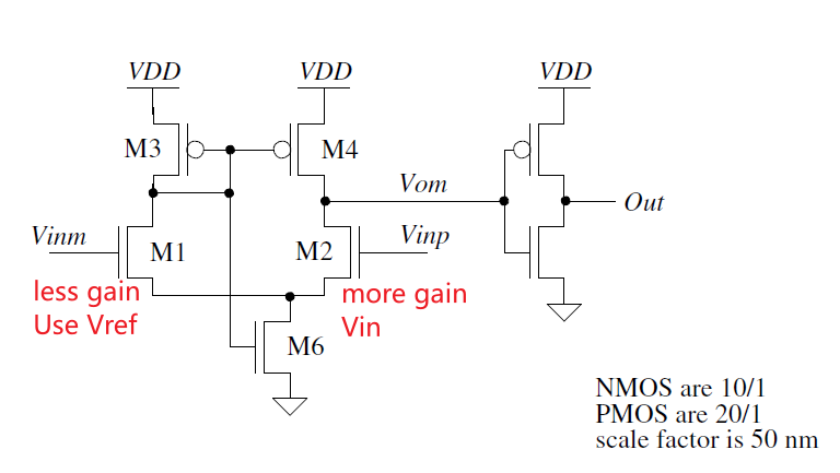
Self-biased Buffer
M3 is diode-connected, 因此 M1 less gain, Use Vref. M2 more gain, Use Vin. It is generally a good idea to connect the reference voltage to the Vinm input.
Peak Detector
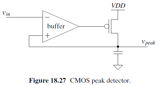
当Vin 接近 Vpeak, MOSFET starts to shut off. 因此电容输出为Vpeak
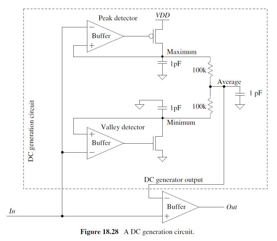
这个电路可以Find the minimum and maximum of input signal
Reduce Buffer Input Resistance
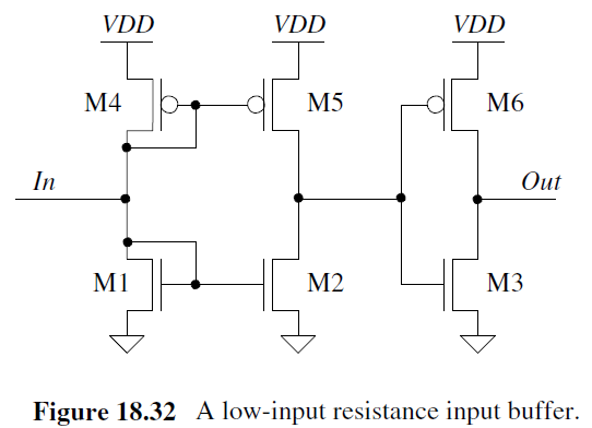
Input swing is limited to a threshold voltage away from the supply voltage.
Charge Pump (Voltage Generator)
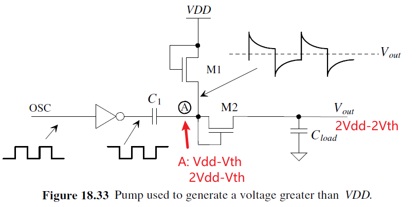
首先意识到: M1, M2 是operate like a diode. 当OSC=VDD, M1 used to pull point A to VDD-Vth. M2只允许A充电到Vout, 不允许从Vout到A. 当OSC=0, A被充电到VDD+(VDD-Vth)=2VDD-Vth. 开启M2, 把Cload充电到2*(VDD- Vth). 实际中C1和Cload 容值相似, 所以需要多次才能把Vout充到设计值
Negative Voltage
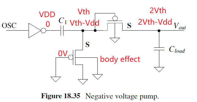
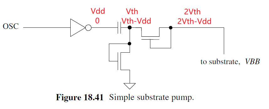
下管把C1右端电压钳位到最大为Vth, Inverter输出=VDD, C1右端电压=Vth, Vout=2Vth. Inverter output=0, C1右端电压降为Vth-Vdd, Vout降为2Vth-Vdd
Using MOSFET for the Capacitors
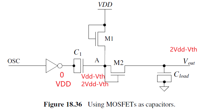
对于MOS Cap 关键是需要Vgs greater than Vth at all possible operating conditions. 而C1作为MOS CAP, 可以满足
Increase the Output Voltage
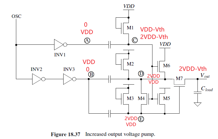
A = 0, C=VDD-Vth, B=VDD
A=VDD, C=2VDD-Vth, 导致 M6 and M5 on, D=VDD, E=VDD.
因此当B=VDD时, D=E=2VDD, Vout=2VDD-Vth. 比之前2VDD-2Vth, 高一个Vth
Generating Higher Voltage: The Dickson Charge Pump
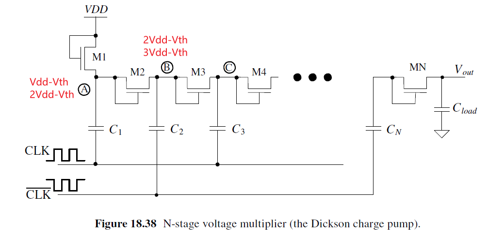
当CLK=0, A=VDD-Vth. 当CLK=VDD, A=2*VDD-Vth, M2 on, B charges to 2VDD-2Vth
当CLK=0, CLK_BAR=VDD, B charges to 3VDD-2Vth.
The output of the multiplier is (N+1)(VDD-Vth)
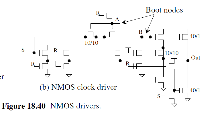
Clock Driver with a Pumped Output Voltage
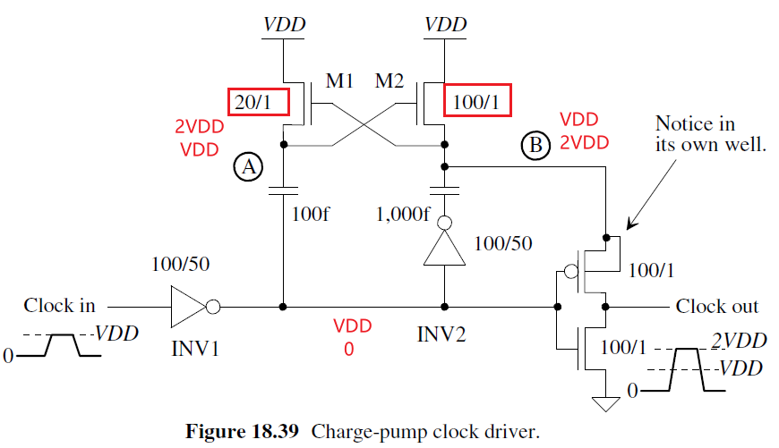
A and B charge to VDD and 2VDD
注意M1的尺寸小, M2的尺寸大. 而且A的电容小,B的电容大. 这是因为A的主要作用是开启M2, 而B是需要提供负载 (Supply power to load).
NMOS Clock Driver
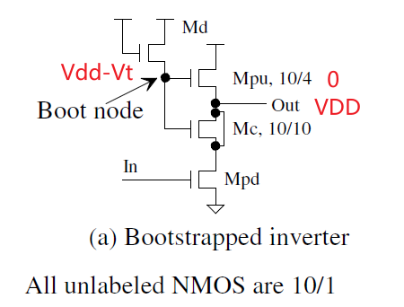
对于没有N-well的情况 (也就是没有PMOS). 只用NMOS做Inverter
Md做为diode, 确保Mpu gate不低于 Vdd-Vth
Mpd的宽长比为Mpu的4倍, 所以Output能close to ground
Mc 做为Cap, 和Md作为Diode, 用来boot the gate of Mpu, 因此Output能达到VDD
为了避免Mpu和Mpd同时 on造成功耗损失, 可用下图结构
Example
在数字电路中, 有一种常见用途就是把substrate接到负电压.
在DRAM中, 把substrate接到 -0.5V ~ -1V. 好处:1, 稳定NMOS的 Vth (变大). 2, increase latch-up immunity after power up. 3, 防止n+ 和p- substrate导通. 4, 允许输入input变负, 也不会导致PN导通. 5, 防止substrate比ground高. 6,减少depletion电容 between n+ and p- substrate. 7, 减少衬底substrate的leakage电流
可用下图电路, 注意substrate本身就是一个大电容, 所以不需要cap了
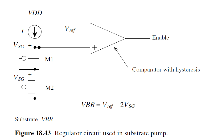
判断substrate电压, 可用下图比较器
VBB+2Vsg=Vref, 只有当VBB高于负值, Enable才为高, 开启charge pump
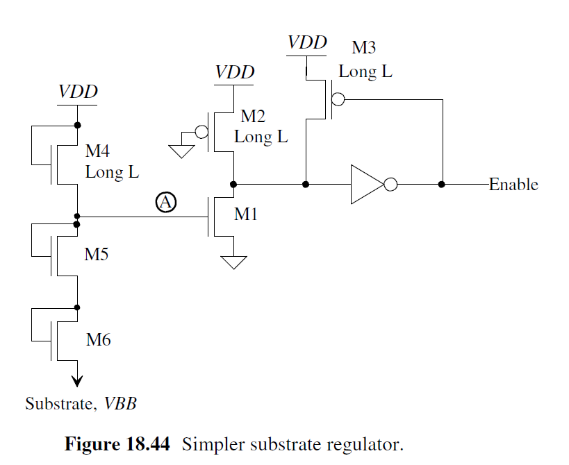
下图为simpler and less accurate implementation of the regulator. 后面是带Hysteresis的比较器, 比较器阈值为Vth
因此Vbb大约被regulate在 -Vth with body effect


 4159
4159

 被折叠的 条评论
为什么被折叠?
被折叠的 条评论
为什么被折叠?
 到【灌水乐园】发言


