


1.与门
module user_and(
input wire a,
input wire b,
output wire out
);

and g1(out,a,b);


endmodule
RTL 结构
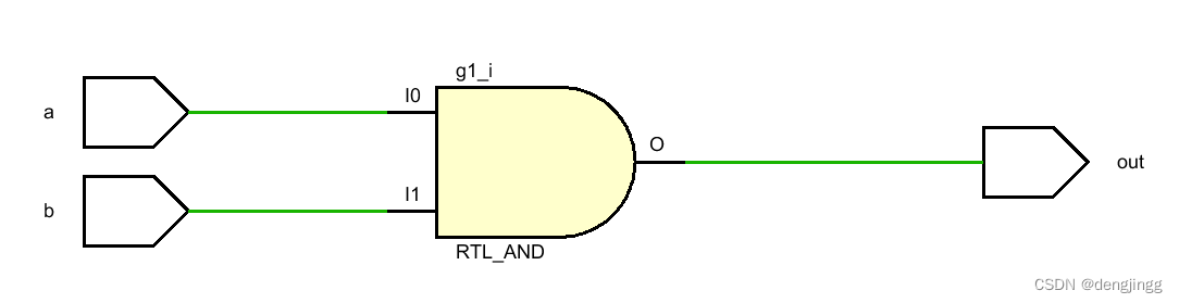
综合后
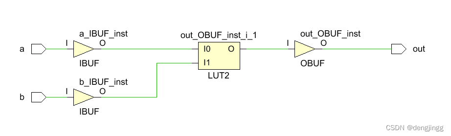
与运算并没有使用什么与门,而是使用了一个LUT,其作用就是一个与关系的真值表
2.自加
a.
`timescale 1ns / 1ps

module self_add(
    input clk,
    output [9:0] tx
    );
    reg [9:0] add;
assign tx = add;
always@(posedge clk) begin
    add <= add +1;
end

endmodule
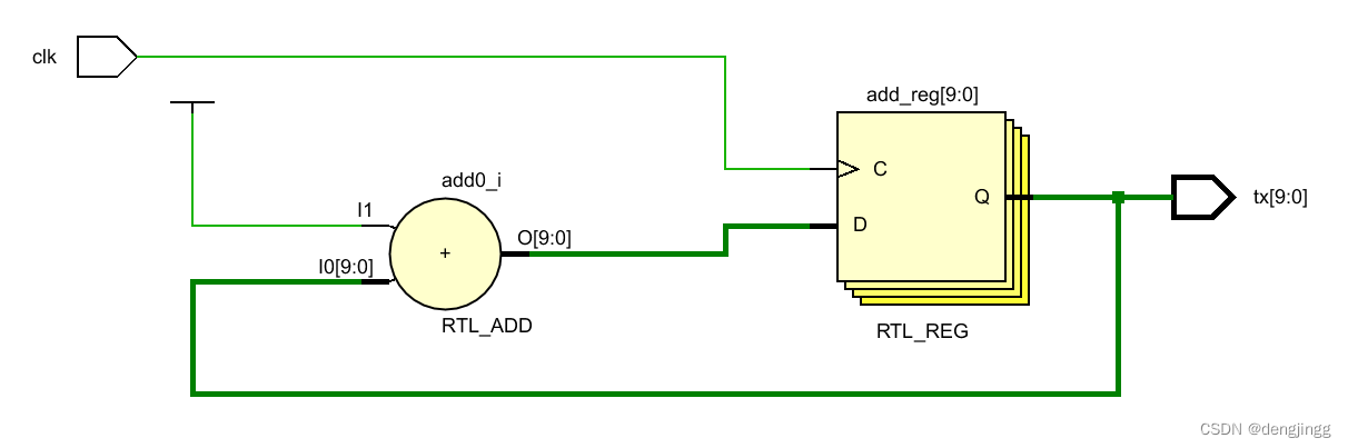 b.累加器复位
module self_add(
    input clk,
    output [9:0] tx
    );
    reg [9:0] add;
assign tx = add;
always@(posedge clk) begin
    if(add == 8)
        add <=0;
    else
        add <= add +1;
end
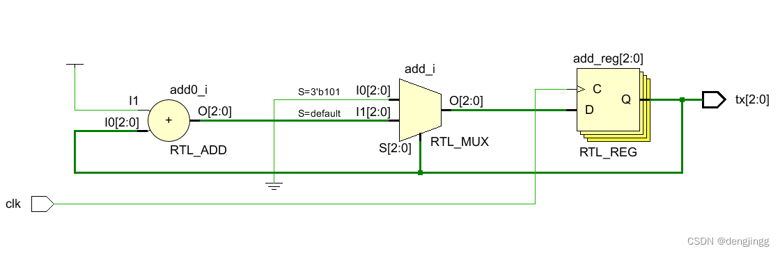
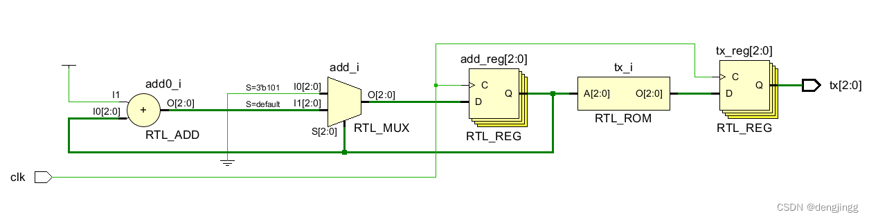
RTL 级别
CNT 的逻辑有两种
1.按照时钟上升沿累加
2.其值为一个值得时候 为 0
所以这样的结构为二路选择器结构 下图 RTL_MUX
if 语句转换成了多路选择器
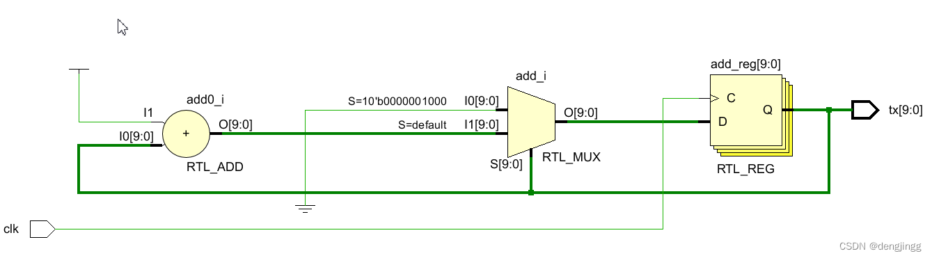
综合,减少寄存器位宽
module self_add(
    input clk,
    output [2:0] tx
    );
    reg [2:0] add;
assign tx = add;
always@(posedge clk) begin
    if(add == 5)
        add <=0;
    else
        add <= add +1;
end

endmodule
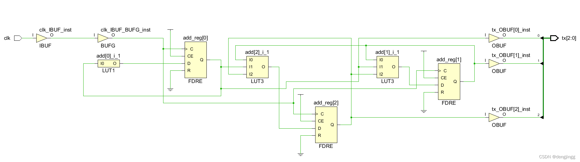
LUT 为查找表 Lookup table,本质上 是在RAM 中做一张增值表
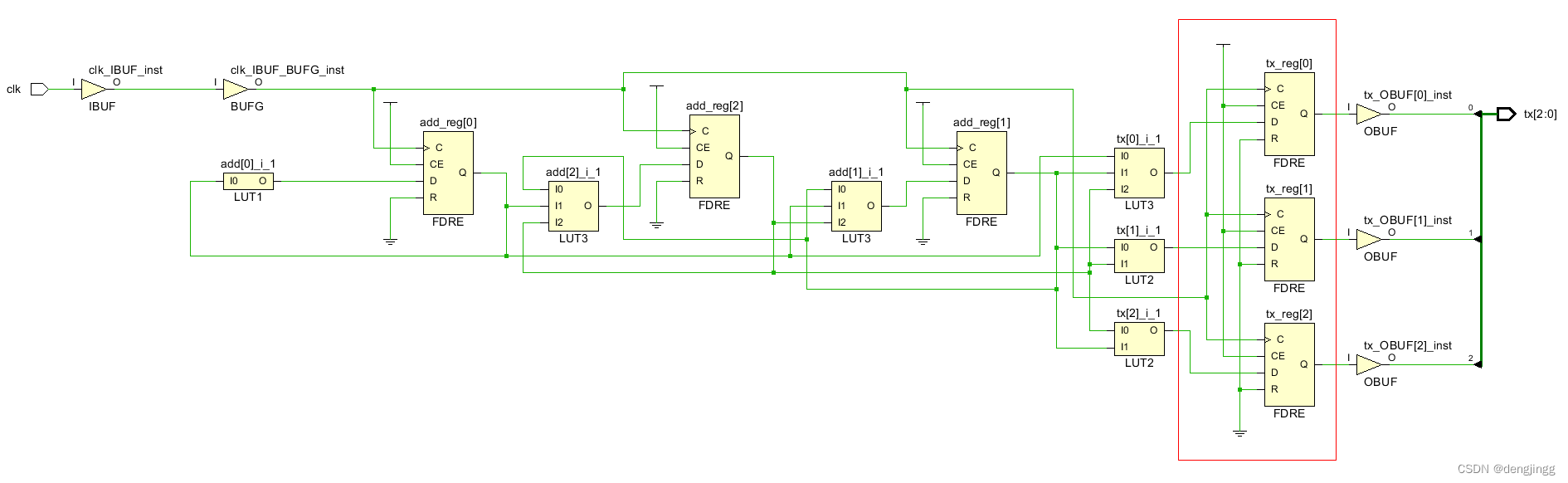
自加器在综合后,其自加功能通过 查找表实现,包括复位值的设定。逻辑关系转换为查找表。
c.给累加器一个初值
`timescale 1ns / 1ps

module self_add(
    input clk,
    output [2:0] tx
    );
    reg [2:0] add;
assign tx = add;
always@(posedge clk) begin
    if(add == 5)
        add <=0;
    else
        add <= add +1;
end
initial add = 4;
endmodule
RTL 分析看不到初值
综合 也是没有变化,初始值的也应该是装入了LUT的逻辑
IO管脚约束后
device 部分有几个标亮的部分
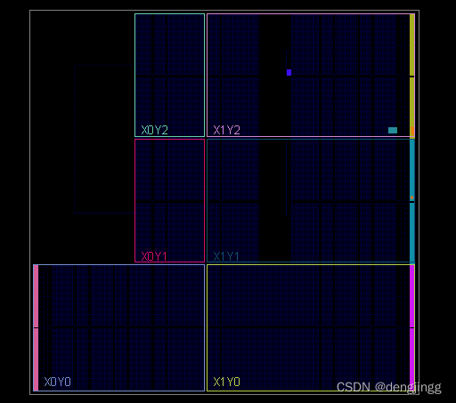
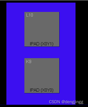
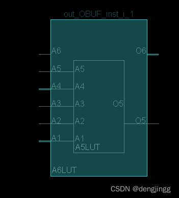
有些A6LUT被电亮,应该是FPGA内部的查找表被使用了
c. 使用case 语句
`timescale 1ns / 1ps

module self_add(
     clk,
     tx
    );
    input clk;
    reg [2:0] add;
    output reg [2:0] tx;

always@(posedge clk) begin
    if(add == 5)
        add <=0;
    else
        add <= add +1;
end
always@(posedge clk) begin
    case(add)
       0:tx <=0;
       1:tx <=1;
       2:tx <=2;
       3:tx <=3;
       4:tx <=4;
       5:tx <=5;
       default:tx <=1;
       endcase
end
initial add = 4;
endmodule
case 关系被转换成 LUT查找表的对应关系
综合
对应关系,产生 LUT 表
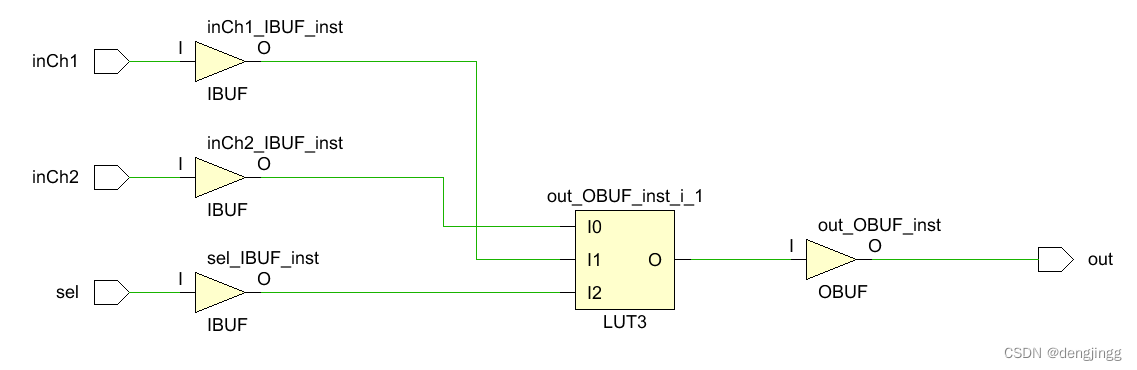
4.多路选择器
module mux
(
    input inCh1,
    input inCh2,
    input sel,
    output out
);

assign out = (sel==0)?inCh1:inCh2;

endmodule
RTL 原理图
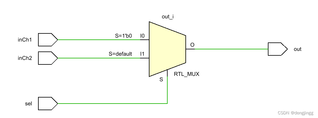
综合后的
不出意外,这里是一个查找表机构
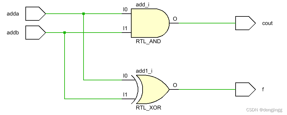
5.半加器
module adder(
    input adda,
    input addb,
    output cout,
    output f
    );

 and add(cout,adda,addb);
 xor add1(f,adda,addb);
endmodule
RTL
综合
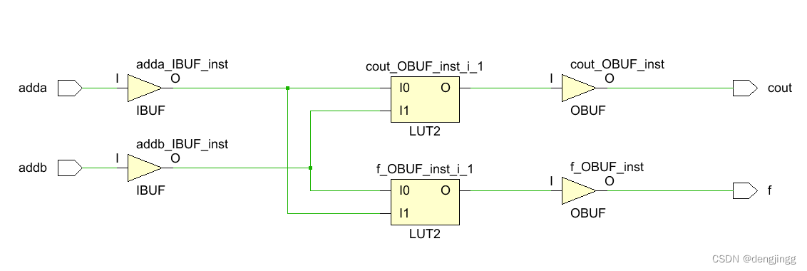
6.全加器,应该也是LUT吧
所以LUT几乎是万能的,所有逻辑关系,与或非等等都可以用查找表表达。
二 使用Verlog 实现 串型数据的发送
使用指定向下的层次
TOP 模块,波特率发生器,tx发送模块
实现上面的模块
1.波特率发生器
`timescale 1ns / 1ns
module baud_clk
(
    input MCLK,
    input G_Reset,
    output reg Buat_CLK
);

parameter F_MCLK = 50000000;
parameter Buad   = 115200;
parameter div    =(F_MCLK/Buad)/2;

reg [25:0] CNT;

always@(posedge MCLK ) begin
    if(G_Reset == 0)
        CNT <= 0;
    else if (CNT ==div )
        CNT <= 0;
    else
        CNT <= CNT + 1;
end

 always@(posedge MCLK ) begin
     if(G_Reset == 0)
         Buat_CLK <= 0;
     else if (CNT == div)
         Buat_CLK <= ~Buat_CLK;
 end
endmodule
2.tx 发送器
`timescale 1ns / 1ps

module uart_logic
(
    input MCLK,
    input G_rest,
    input Buad_CLK,
    input send,
    output reg tx
);

reg [7:0] data = 8'b0101_0010;
reg [3:0] state = 0;
reg work = 0;

always@(posedge Buad_CLK)
begin
    if(G_rest==0 || state ==11)
       work <= 0;
    else if(send==1 && work ==0)
       work <=1;
end

always@(negedge work)
begin
data <= data +1;
end

always@(posedge Buad_CLK)
begin
    if(G_rest == 0)
        state <= 0;
    else if(state == 11)
        state <= 0;
    else if(work)
        state <= state + 1;
end

always@(posedge Buad_CLK)
begin
    if(G_rest == 0)
        tx <= 1;
    else
        case(state)
         0:  tx <= 1;
         1:  tx <= 0;
         2:  tx <= data[0];
         3:  tx <= data[1];
         4:  tx <= data[2];
         5:  tx <= data[3];
         6:  tx <= data[4];
         7:  tx <= data[5];
         8:  tx <= data[6];
         9:  tx <= data[7];
         10:  tx <= 1;
         11: tx <= 1;
       default: tx <= 1;
       endcase
end
endmodule
3.Top
`timescale 1ns / 1ps

module uart_top
(
    input MCLK,
    input send,
    input reset,
    output tx
);
wire buad;
baud_clk baud_1
(
    .MCLK(MCLK),
    .G_Reset(reset),
    .Buat_CLK(buad)
);
uart_logic logic_1
(
    .MCLK(MCLK),
    .G_rest(reset),
    .Buad_CLK(buad),
    .send(~send),
    .tx(tx)
);
endmodule
RTL分析
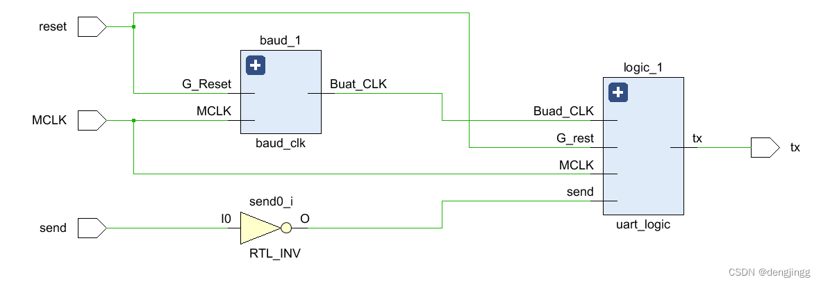
综合分析
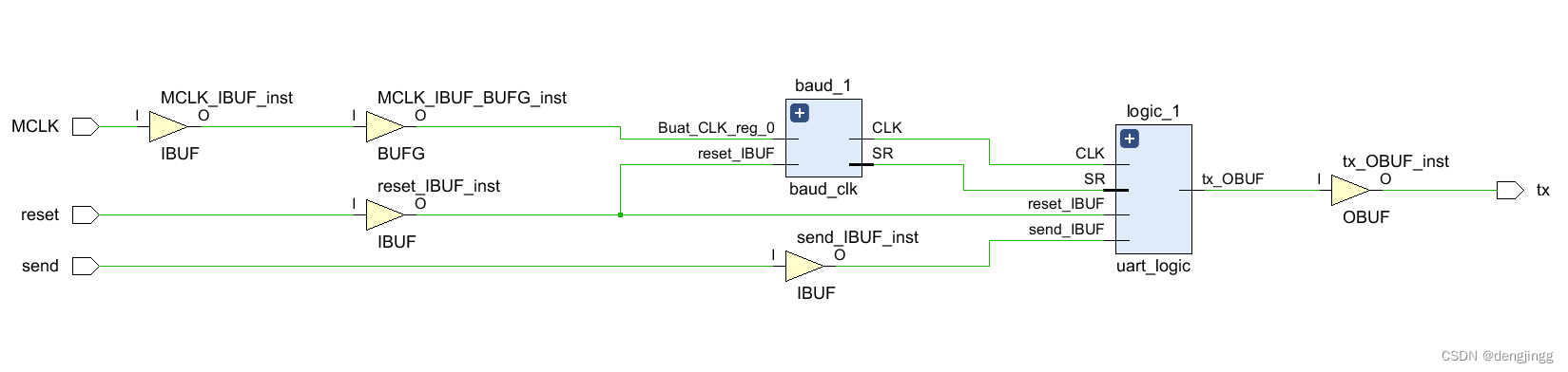
三角形的BUF 是一个缓冲器,提高信号的传递扇出能力。
道这里已经无法展开了,太多的结构眼花缭乱。
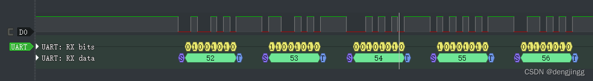
最后用逻辑分析仪查看输出数据
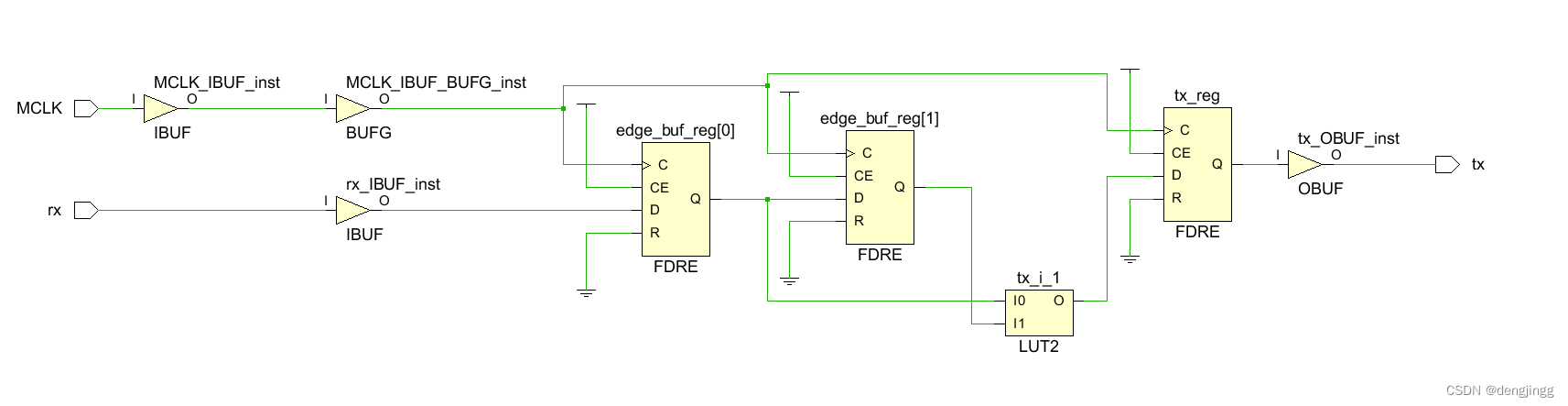
边沿检测
module edge_11
(
    input MCLK,
    input rx,
    output reg tx

);

reg [1:0] edge_buf;

always@(posedge MCLK)
begin
    edge_buf[0] <= rx;
    edge_buf[1] <= edge_buf[0];

end

always@(posedge MCLK)
begin
    if(edge_buf == 2'b01)
        tx <= 1;
    else
        tx <=0;
end

endmodule


 3286
3286


 被折叠的 条评论
为什么被折叠?
被折叠的 条评论
为什么被折叠?
 到【灌水乐园】发言


