


文章目录
- 前言
- 硬件
- 软件
- 结构体
- SRAM_HandleTypeDef
- FMC_NORSRAM_InitTypeDef
- NSBank(SRAM内存块选择)
- DataAddressMux(数据地址总线)
- MemoryType(存储器类型)
- MemoryDataWidth(存储器数据总线宽度)
- BurstAccessMode(突发模式)
- WaitSignalPolarity(等待信号极性)
- WrapMode(回卷模式)
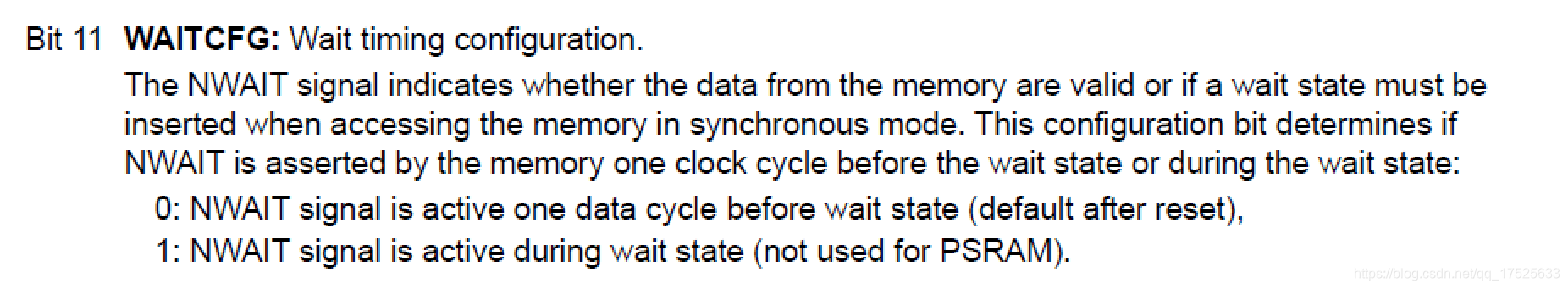
- WaitSignalActive(等待时序配置)
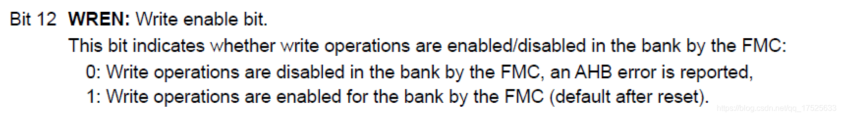
- WriteOperation(写操作)
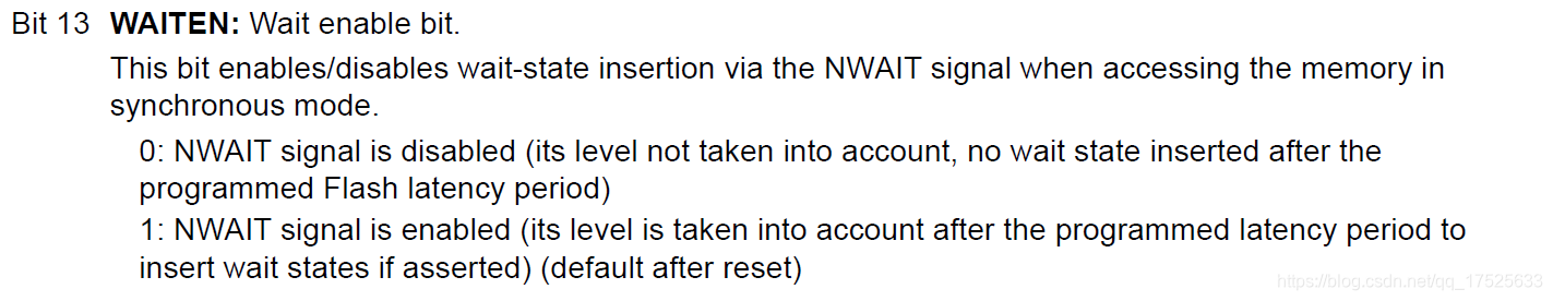
- WaitSignal(等待使能)
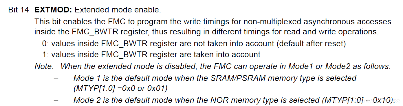
- ExtendedMode(拓展模式)
- AsynchronousWait(同步传输等待)
- WriteBurst(写突发使能)
- ContinuousClock(连续时钟)
- WriteFifo(写队列)
- PageSize(页容量)
- FMC_NORSRAM_TimingTypeDef
- 程序
前言
本文主要介绍F429通过SRAM并口模块驱动MCU显示屏的实验详解,这部分涉及以下部分知识:
- MCU显示屏
- SRAM并口——FMC 的原理及HAL库的实现
该实验实现的功能为,每经过1秒中,执行一次以下操作:
- LED灯反转一次。
- 屏幕背景颜色变化一次。
且 在屏幕上 用不同字号显示一串信息。
硬件
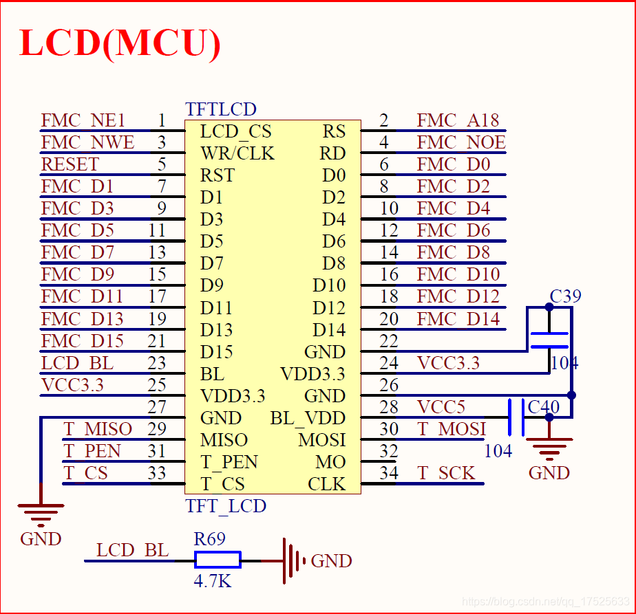
硬件连接部分:
- 16位数据总线——写入读取数据
- A18——写入命令/数据
- NE1——片选信号
- NWE——写信号
- NOE——读信号
- BL——背光使能
软件
结构体
SRAM_HandleTypeDef
/**
  * @brief  SRAM handle Structure definition
  */
#if (USE_HAL_SRAM_REGISTER_CALLBACKS == 1)
typedef struct __SRAM_HandleTypeDef
#else
typedef struct
#endif /* USE_HAL_SRAM_REGISTER_CALLBACKS  */
{
  FMC_NORSRAM_TypeDef           *Instance;  /*!< Register base address                        */

  FMC_NORSRAM_EXTENDED_TypeDef  *Extended;  /*!< Extended mode register base address          */

  FMC_NORSRAM_InitTypeDef       Init;       /*!< SRAM device control configuration parameters */

  HAL_LockTypeDef               Lock;       /*!< SRAM locking object                          */

  __IO HAL_SRAM_StateTypeDef    State;      /*!< SRAM device access state                     */

  DMA_HandleTypeDef             *hdma;      /*!< Pointer DMA handler                          */

#if (USE_HAL_SRAM_REGISTER_CALLBACKS == 1)
  void  (* MspInitCallback)        ( struct __SRAM_HandleTypeDef * hsram);    /*!< SRAM Msp Init callback              */
  void  (* MspDeInitCallback)      ( struct __SRAM_HandleTypeDef * hsram);    /*!< SRAM Msp DeInit callback            */
  void  (* DmaXferCpltCallback)    ( DMA_HandleTypeDef * hdma);               /*!< SRAM DMA Xfer Complete callback     */
  void  (* DmaXferErrorCallback)   ( DMA_HandleTypeDef * hdma);               /*!< SRAM DMA Xfer Error callback        */
#endif
} SRAM_HandleTypeDef;
Instance(FMC寄存器地址)
此处可以认为是固定值:
#define FMC_NORSRAM_DEVICE FMC_Bank1
具体的取值为:
#define FMC_R_BASE 0xA0000000UL /*!< FMC registers base address */
这是FMC的寄存器地址分配:

Extended(拓展寄存器地址)
#define FMC_NORSRAM_EXTENDED_DEVICE FMC_Bank1E
此处对应拓展寄存器,该部分地址为:
#define FMC_Bank1E_R_BASE (FMC_R_BASE + 0x0104UL)

Init(初始化变量)
结构体FMC_NORSRAM_InitTypeDef变量。详细见后文。
Lock(锁)
取值为:
/**
  * @brief  HAL Lock structures definition
  */
typedef enum
{
  HAL_UNLOCKED = 0x00U,
  HAL_LOCKED   = 0x01U
} HAL_LockTypeDef;
State(状态)
取值范围为:
/**
  * @brief  HAL SRAM State structures definition
  */
typedef enum
{
  HAL_SRAM_STATE_RESET     = 0x00U,  /*!< SRAM not yet initialized or disabled           */
  HAL_SRAM_STATE_READY     = 0x01U,  /*!< SRAM initialized and ready for use             */
  HAL_SRAM_STATE_BUSY      = 0x02U,  /*!< SRAM internal process is ongoing               */
  HAL_SRAM_STATE_ERROR     = 0x03U,  /*!< SRAM error state                               */
  HAL_SRAM_STATE_PROTECTED = 0x04U   /*!< SRAM peripheral NORSRAM device write protected */

} HAL_SRAM_StateTypeDef;
hdma(dma句柄)
暂时不用
FMC_NORSRAM_InitTypeDef
/**
  * @brief  FMC NORSRAM Configuration Structure definition
  */
typedef struct
{
  uint32_t NSBank;                       /*!< Specifies the NORSRAM memory device that will be used.
                                              This parameter can be a value of @ref FMC_NORSRAM_Bank                     */

  uint32_t DataAddressMux;               /*!< Specifies whether the address and data values are
                                              multiplexed on the data bus or not.
                                              This parameter can be a value of @ref FMC_Data_Address_Bus_Multiplexing    */

  uint32_t MemoryType;                   /*!< Specifies the type of external memory attached to
                                              the corresponding memory device.
                                              This parameter can be a value of @ref FMC_Memory_Type                      */

  uint32_t MemoryDataWidth;              /*!< Specifies the external memory device width.
                                              This parameter can be a value of @ref FMC_NORSRAM_Data_Width               */

  uint32_t BurstAccessMode;              /*!< Enables or disables the burst access mode for Flash memory,
                                              valid only with synchronous burst Flash memories.
                                              This parameter can be a value of @ref FMC_Burst_Access_Mode                */

  uint32_t WaitSignalPolarity;           /*!< Specifies the wait signal polarity, valid only when accessing
                                              the Flash memory in burst mode.
                                              This parameter can be a value of @ref FMC_Wait_Signal_Polarity             */

  uint32_t WrapMode;                     /*!< Enables or disables the Wrapped burst access mode for Flash
                                              memory, valid only when accessing Flash memories in burst mode.
                                              This parameter can be a value of @ref FMC_Wrap_Mode
                                              This mode is not available for the STM32F446/467/479xx devices                    */

  uint32_t WaitSignalActive;             /*!< Specifies if the wait signal is asserted by the memory one
                                              clock cycle before the wait state or during the wait state,
                                              valid only when accessing memories in burst mode.
                                              This parameter can be a value of @ref FMC_Wait_Timing                      */

  uint32_t WriteOperation;               /*!< Enables or disables the write operation in the selected device by the FMC.
                                              This parameter can be a value of @ref FMC_Write_Operation                  */

  uint32_t WaitSignal;                   /*!< Enables or disables the wait state insertion via wait
                                              signal, valid for Flash memory access in burst mode.
                                              This parameter can be a value of @ref FMC_Wait_Signal                      */

  uint32_t ExtendedMode;                 /*!< Enables or disables the extended mode.
                                              This parameter can be a value of @ref FMC_Extended_Mode                    */

  uint32_t AsynchronousWait;             /*!< Enables or disables wait signal during asynchronous transfers,
                                              valid only with asynchronous Flash memories.
                                              This parameter can be a value of @ref FMC_AsynchronousWait                 */

  uint32_t WriteBurst;                   /*!< Enables or disables the write burst operation.
                                              This parameter can be a value of @ref FMC_Write_Burst                      */

  uint32_t ContinuousClock;              /*!< Enables or disables the FMC clock output to external memory devices.
                                              This parameter is only enabled through the FMC_BCR1 register, and don't care
                                              through FMC_BCR2..4 registers.
                                              This parameter can be a value of @ref FMC_Continous_Clock                  */

  uint32_t WriteFifo;                    /*!< Enables or disables the write FIFO used by the FMC controller.
                                              This parameter is only enabled through the FMC_BCR1 register, and don't care
                                              through FMC_BCR2..4 registers.
                                              This parameter can be a value of @ref FMC_Write_FIFO
                                              This mode is available only for the STM32F446/469/479xx devices            */

  uint32_t PageSize;                     /*!< Specifies the memory page size.
                                              This parameter can be a value of @ref FMC_Page_Size                        */
}FMC_NORSRAM_InitTypeDef;
NSBank(SRAM内存块选择)
/** @defgroup FMC_NORSRAM_Bank FMC NOR/SRAM Bank
  * @{
  */
#define FMC_NORSRAM_BANK1                       0x00000000U
#define FMC_NORSRAM_BANK2                       0x00000002U
#define FMC_NORSRAM_BANK3                       0x00000004U
#define FMC_NORSRAM_BANK4                       0x00000006U
/**
  * @}
  */
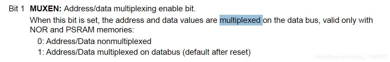
DataAddressMux(数据地址总线)
该位用于配置数据与地址是否共用一条总线,选项如下:
/** @defgroup FMC_Data_Address_Bus_Multiplexing FMC Data Address Bus Multiplexing
  * @{
  */
#define FMC_DATA_ADDRESS_MUX_DISABLE            0x00000000U
#define FMC_DATA_ADDRESS_MUX_ENABLE             0x00000002U
/**
  * @}
  */
对应寄存器选择如下:
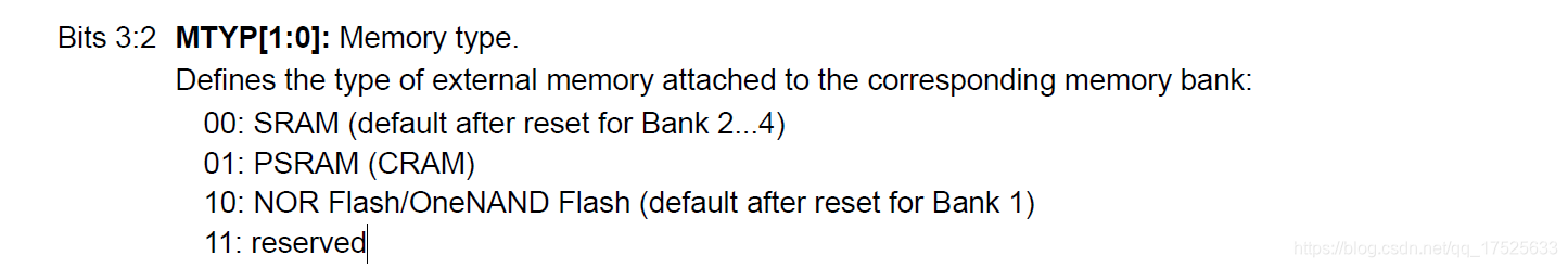
MemoryType(存储器类型)
该寄存器用于指定存储器的类型:
/** @defgroup FMC_Memory_Type FMC Memory Type
  * @{
  */
#define FMC_MEMORY_TYPE_SRAM                    0x00000000U
#define FMC_MEMORY_TYPE_PSRAM                   0x00000004U
#define FMC_MEMORY_TYPE_NOR                     0x00000008U
/**
  * @}
  */
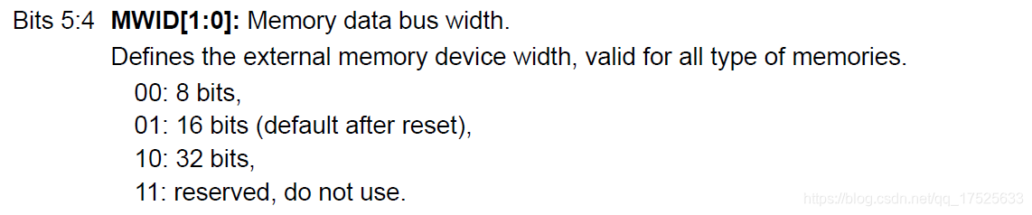
MemoryDataWidth(存储器数据总线宽度)
该成员用于指定存储器的总线数据宽度:
/** @defgroup FMC_NORSRAM_Data_Width FMC NORSRAM Data Width
  * @{
  */
#define FMC_NORSRAM_MEM_BUS_WIDTH_8             0x00000000U
#define FMC_NORSRAM_MEM_BUS_WIDTH_16            0x00000010U
#define FMC_NORSRAM_MEM_BUS_WIDTH_32            0x00000020U
/**
  * @}
  */
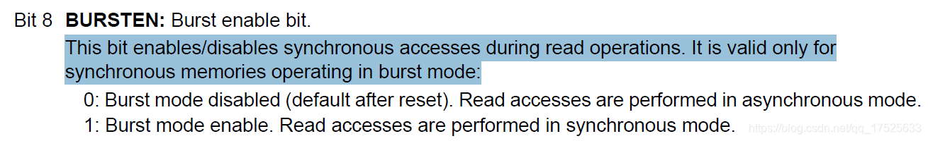
BurstAccessMode(突发模式)
/** @defgroup FMC_Burst_Access_Mode FMC Burst Access Mode
  * @{
  */
#define FMC_BURST_ACCESS_MODE_DISABLE           0x00000000U
#define FMC_BURST_ACCESS_MODE_ENABLE            0x00000100U
/**
  * @}
  */
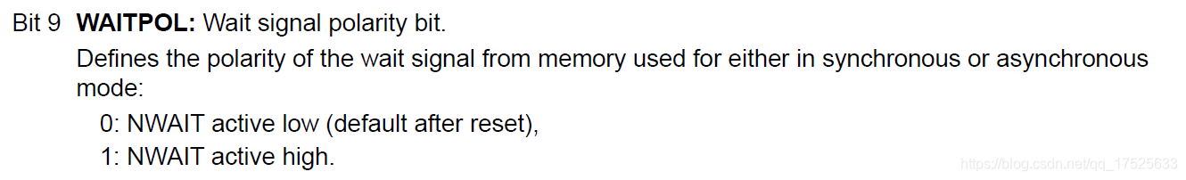
WaitSignalPolarity(等待信号极性)
/** @defgroup FMC_Wait_Signal_Polarity FMC Wait Signal Polarity
  * @{
  */
#define FMC_WAIT_SIGNAL_POLARITY_LOW            0x00000000U
#define FMC_WAIT_SIGNAL_POLARITY_HIGH           0x00000200U
/**
  * @}
  */
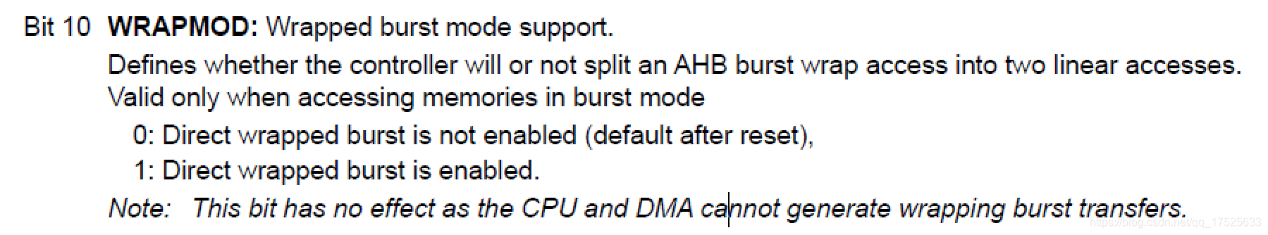
WrapMode(回卷模式)
/** @defgroup FMC_Wrap_Mode FMC Wrap Mode
  * @{
  */
/** @note This mode is not available for the STM32F446/469/479xx devices
  */
#define FMC_WRAP_MODE_DISABLE                   0x00000000U
#define FMC_WRAP_MODE_ENABLE                    0x00000400U
/**
  * @}
  */
WaitSignalActive(等待时序配置)
/** @defgroup FMC_Wait_Timing FMC Wait Timing
  * @{
  */
#define FMC_WAIT_TIMING_BEFORE_WS               0x00000000U
#define FMC_WAIT_TIMING_DURING_WS               0x00000800U
/**
  * @}
  */
WriteOperation(写操作)
写操作使能
/** @defgroup FMC_Write_Operation FMC Write Operation
  * @{
  */
#define FMC_WRITE_OPERATION_DISABLE             0x00000000U
#define FMC_WRITE_OPERATION_ENABLE              0x00001000U
/**
  * @}
  */
WaitSignal(等待使能)
/** @defgroup FMC_Wait_Signal FMC Wait Signal
  * @{
  */
#define FMC_WAIT_SIGNAL_DISABLE                 0x00000000U
#define FMC_WAIT_SIGNAL_ENABLE                  0x00002000U
/**
  * @}
  */
ExtendedMode(拓展模式)
/** @defgroup FMC_Extended_Mode FMC Extended Mode
  * @{
  */
#define FMC_EXTENDED_MODE_DISABLE               0x00000000U
#define FMC_EXTENDED_MODE_ENABLE                0x00004000U
/**
  * @}
  */
AsynchronousWait(同步传输等待)
/** @defgroup FMC_AsynchronousWait FMC Asynchronous Wait
  * @{
  */
#define FMC_ASYNCHRONOUS_WAIT_DISABLE           0x00000000U
#define FMC_ASYNCHRONOUS_WAIT_ENABLE            0x00008000U
/**
  * @}
  */
WriteBurst(写突发使能)
/** @defgroup FMC_Write_Burst FMC Write Burst
  * @{
  */
#define FMC_WRITE_BURST_DISABLE                 0x00000000U
#define FMC_WRITE_BURST_ENABLE                  0x00080000U
/**
  * @}
  */
ContinuousClock(连续时钟)
/** @defgroup FMC_Continous_Clock FMC Continuous Clock
  * @{
  */
#define FMC_CONTINUOUS_CLOCK_SYNC_ONLY          0x00000000U
#define FMC_CONTINUOUS_CLOCK_SYNC_ASYNC         0x00100000U
/**
  * @}
  */
/** @defgroup FMC_Write_FIFO FMC Write FIFO
  * @note  These values are available only for the STM32F446/469/479xx devices.
  * @{
  */
#define FMC_WRITE_FIFO_DISABLE           ((uint32_t)FMC_BCR1_WFDIS)
#define FMC_WRITE_FIFO_ENABLE            0x00000000U
/**
  * @}
  */
WriteFifo(写队列)
/** @defgroup FMC_Write_FIFO FMC Write FIFO
  * @note  These values are available only for the STM32F446/469/479xx devices.
  * @{
  */
#define FMC_WRITE_FIFO_DISABLE           ((uint32_t)FMC_BCR1_WFDIS)
#define FMC_WRITE_FIFO_ENABLE            0x00000000U
/**
  * @}
  */
此处有点问题FMC_BCR1_WFDIS没有找到定义。该成员在F429中无效。
PageSize(页容量)
/** @defgroup FMC_Page_Size FMC Page Size
  * @{
  */
#define FMC_PAGE_SIZE_NONE           0x00000000U
#define FMC_PAGE_SIZE_128            ((uint32_t)FMC_BCR1_CPSIZE_0)
#define FMC_PAGE_SIZE_256            ((uint32_t)FMC_BCR1_CPSIZE_1)
#define FMC_PAGE_SIZE_512            ((uint32_t)(FMC_BCR1_CPSIZE_0 | FMC_BCR1_CPSIZE_1))
#define FMC_PAGE_SIZE_1024           ((uint32_t)FMC_BCR1_CPSIZE_2)
/**
  * @}
  */
FMC_NORSRAM_TimingTypeDef
/**
* @brief FMC NORSRAM Timing parameters structure definition
*/
typedef struct
{
uint32_t AddressSetupTime; /*!< Defines the number of HCLK cycles to configure
the duration of the address setup time.
This parameter can be a value between Min_Data = 0 and Max_Data = 15.
@note This parameter is not used with synchronous NOR Flash memories. */
uint32_t AddressHoldTime; /*!< Defines the number of HCLK cycles to configure
the duration of the address hold time.
This parameter can be a value between Min_Data = 1 and Max_Data = 15.
@note This parameter is not used with synchronous NOR Flash memories. */
uint32_t DataSetupTime; /*!< Defines the number of HCLK cycles to configure
the duration of the data setup time.
This parameter can be a value between Min_Data = 1 and Max_Data = 255.
@note This parameter is used for SRAMs, ROMs and asynchronous multiplexed
NOR Flash memories. */
uint32_t BusTurnAroundDuration; /*!< Defines the number of HCLK cycles to configure
the duration of the bus turnaround.
This parameter can be a value between Min_Data = 0 and Max_Data = 15.
@note This parameter is only used for multiplexed NOR Flash memories. */
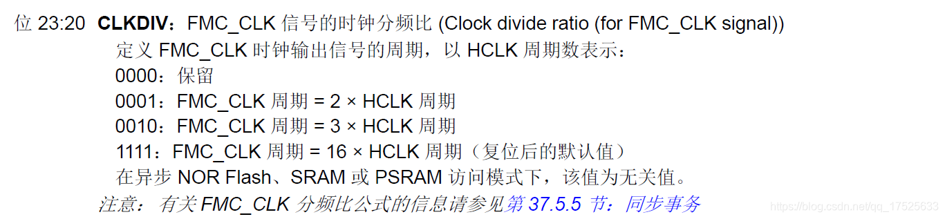
uint32_t CLKDivision; /*!< Defines the period of CLK clock output signal, expressed in number of
HCLK cycles. This parameter can be a value between Min_Data = 2 and Max_Data = 16.
@note This parameter is not used for asynchronous NOR Flash, SRAM or ROM
accesses. */
uint32_t DataLatency; /*!< Defines the number of memory clock cycles to issue
to the memory before getting the first data.
The parameter value depends on the memory type as shown below:
- It must be set to 0 in case of a CRAM
- It is don't care in asynchronous NOR, SRAM or ROM accesses
- It may assume a value between Min_Data = 2 and Max_Data = 17 in NOR Flash memories
with synchronous burst mode enable */
uint32_t AccessMode; /*!< Specifies the asynchronous access mode.
This parameter can be a value of @ref FMC_Access_Mode */
}FMC_NORSRAM_TimingTypeDef;
AddressSetupTime(地址建立时间)
取值范围为:[0-15]。
AddressHoldTime(地址保持时间)
该值取值范围为:[1-15]。
DataSetupTime(数据建立时间)
取值范围:[1-255]
BusTurnAroundDuration(总线周转时间)
取值范围:[0-15]
CLKDivision(时钟分频比)
取值范围[2-16]
DataLatency(数据延时)
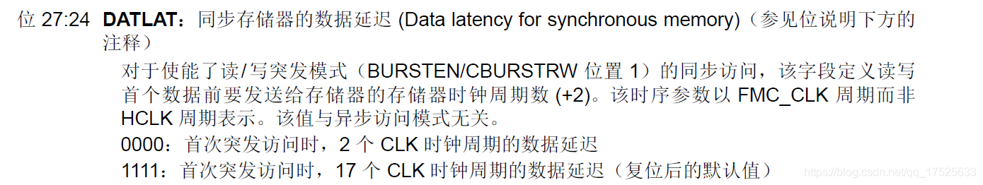
异步方式此数据无所谓。
AccessMode(访问模式)
/** @defgroup FMC_Access_Mode FMC Access Mode
  * @{
  */
#define FMC_ACCESS_MODE_A                        0x00000000U
#define FMC_ACCESS_MODE_B                        0x10000000U
#define FMC_ACCESS_MODE_C                        0x20000000U
#define FMC_ACCESS_MODE_D                        0x30000000U
/**
  * @}
  */
程序
主程序
int main(void)
{
    /* 1.定义变量 */
    u8 x = 0;
    u8 lcd_id[12];

    /* 2.硬件初始化 */
    HAL_Init();                      //初始化HAL库
    Stm32_Clock_Init(360, 25, 2, 8); //设置时钟,180Mhz
    delay_init(180);                 //初始化延时函数
    uart_init(115200);               //初始化USART
    LED_Init();                      //初始化LED
    LCD_Init();                      //初始化LCD

    /* 3.功能初始化 */
    POINT_COLOR = RED;
    sprintf((char *)lcd_id, "LCD ID:%04X", lcddev.id); //将LCD ID打印到lcd_id数组。

    /* 4.while循环 */
    while (1)
    {
        switch (x)
        {
        case 0:
            LCD_Clear(WHITE);
            break;
        case 1:
            LCD_Clear(BLACK);
            break;
        case 2:
            LCD_Clear(BLUE);
            break;
        case 3:
            LCD_Clear(RED);
            break;
        case 4:
            LCD_Clear(MAGENTA);
            break;
        case 5:
            LCD_Clear(GREEN);
            break;
        case 6:
            LCD_Clear(CYAN);
            break;
        case 7:
            LCD_Clear(YELLOW);
            break;
        case 8:
            LCD_Clear(BRRED);
            break;
        case 9:
            LCD_Clear(GRAY);
            break;
        case 10:
            LCD_Clear(LGRAY);
            break;
        case 11:
            LCD_Clear(BROWN);
            break;
        }
        POINT_COLOR = RED;
        LCD_ShowString(10, 40, 240, 32, 32, "Apollo STM32F4/F7");
        LCD_ShowString(10, 80, 240, 24, 24, "TFTLCD TEST");
        LCD_ShowString(10, 110, 240, 16, 16, "ATOM@ALIENTEK");
        LCD_ShowString(10, 130, 240, 16, 16, lcd_id); //显示LCD ID
        LCD_ShowString(10, 150, 240, 12, 12, "2016/1/6");
        x++;
        if (x == 12)
            x = 0;
        LED0 = !LED0;
        delay_ms(1000);
    }
}
主程序主要分成四个部分:
- 变量初始化
- 硬件初始化
- 功能初始化
- while循环
在硬件初始化中,与本文相关的内容为LCD初始化函数LCD_Init()。该函数会在后文详细介绍。其余硬件已在前面的博文中介绍,此处不再详细列出。
在功能初始化中,主要将文字的颜色设置为红色,且将产品的ID打印到串口中。
在while循环中,每一秒钟执行一次。分别将屏幕的背景颜色修改一次,显示不同大小的字体以及闪烁LED灯。
配置程序
由于本文程序量比较大,本文分块介绍重点实现原理,而不是程序逐条分析,大致分成以下几个部分:
- 指令与数据——分析如何区分35510的指令与数据
- FMC初始化HAL实现方式
指令与数据
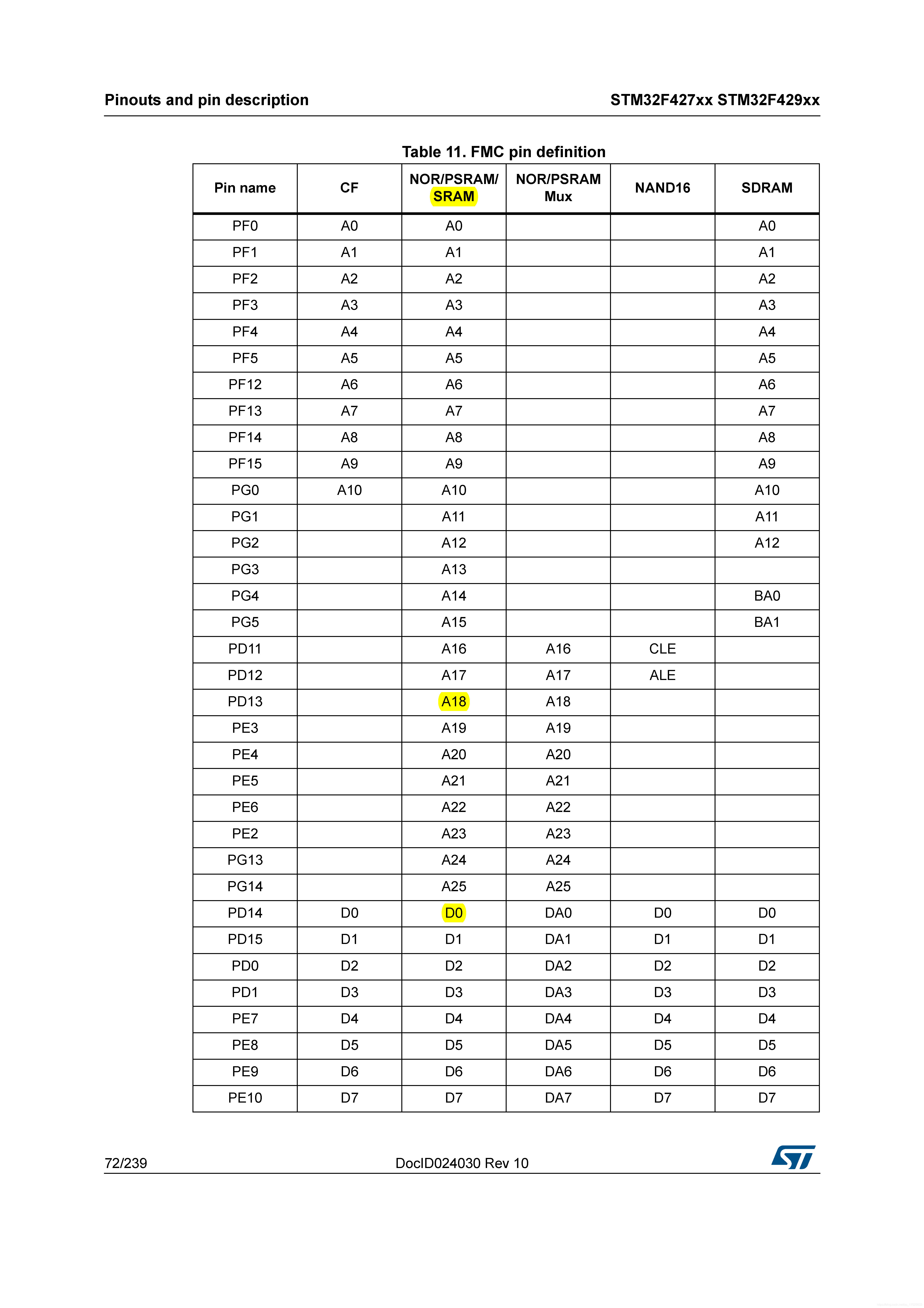
在35510屏幕中D/CX管脚区分接收的是指令还是数据,该管脚在硬件上与ARM的A18管脚相连。所以,可以得知:
- 当A18管脚为低电平时,D/CX为低电平,写入的数据为指令。
- 当A18管脚为高电平时,D/CX为高电平,写入的数据为数据。
在35510的数据宽度为16位,所以,ARM的数据总线宽度采用16位。因此,ARM的A18管脚实际上对应的编址为第19位。因此,可以得到:当地址小于2^19(0x80000)时,写入的数据为指令,地址大于0x80000时,写入的数据为数据。可以总结如下:
因此,可以采用一个边界值附近,取0x7FFFE为指令,0x80000为数据。具体实现方式如下:
//LCD地址结构体
typedef struct
{
vu16 LCD_REG; //A18为低
vu16 LCD_RAM; //A18位高
} LCD_TypeDef;
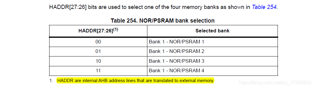
//使用NOR/SRAM的 Bank1.sector1,地址位HADDR[27,26]=00 A18作为数据命令区分线
//注意设置时STM32内部会右移一位对其!
#define LCD_BASE ((u32)(0x60000000 | 0x0007FFFE))
#define LCD ((LCD_TypeDef *)LCD_BASE)
通过以上定义,可以得到:
LCD->LCD_REG//对应地址为0x7FFFE,即为指令
LCD->LCD_RAM//对应地址为0x80000,即为数据
而使用的模块为FMC中的SRAM,所以,其增加一个偏移地址为:0x60000000。
这样,下面的函数就很容易理解:
//写寄存器函数
//regval:寄存器值
void LCD_WR_REG(vu16 regval)
{
    regval = regval;       //使用-O2优化的时候,必须插入的延时
    LCD->LCD_REG = regval; //写入要写的寄存器序号
}
//写LCD数据
//data:要写入的值
void LCD_WR_DATA(vu16 data)
{
    data = data; //使用-O2优化的时候,必须插入的延时
    LCD->LCD_RAM = data;
}
//读LCD数据
//返回值:读到的值
u16 LCD_RD_DATA(void)
{
    vu16 ram; //防止被优化
    ram = LCD->LCD_RAM;
    return ram;
}
//写寄存器
//LCD_Reg:寄存器地址
//LCD_RegValue:要写入的数据
void LCD_WriteReg(u16 LCD_Reg, u16 LCD_RegValue)
{
    LCD->LCD_REG = LCD_Reg;      //写入要写的寄存器序号
    LCD->LCD_RAM = LCD_RegValue; //写入数据
}
//读寄存器
//LCD_Reg:寄存器地址
//返回值:读到的数据
u16 LCD_ReadReg(u16 LCD_Reg)
{
    LCD_WR_REG(LCD_Reg); //写入要读的寄存器序号
    delay_us(5);
    return LCD_RD_DATA(); //返回读到的值
}
//开始写GRAM
void LCD_WriteRAM_Prepare(void)
{
    LCD->LCD_REG = lcddev.wramcmd;
}
//LCD写GRAM
//RGB_Code:颜色值
void LCD_WriteRAM(u16 RGB_Code)
{
    LCD->LCD_RAM = RGB_Code; //写十六位GRAM
}
SRAM初始化
HAL_SRAM_Init
/**
  * @brief  Performs the SRAM device initialization sequence
  * @param  hsram pointer to a SRAM_HandleTypeDef structure that contains
  *                the configuration information for SRAM module.
  * @param  Timing Pointer to SRAM control timing structure
  * @param  ExtTiming Pointer to SRAM extended mode timing structure
  * @retval HAL status
  */
HAL_StatusTypeDef HAL_SRAM_Init(SRAM_HandleTypeDef *hsram, FMC_NORSRAM_TimingTypeDef *Timing, FMC_NORSRAM_TimingTypeDef *ExtTiming)
{
  /* Check the SRAM handle parameter */
  if(hsram == NULL)
  {
     return HAL_ERROR;
  }

  if(hsram->State == HAL_SRAM_STATE_RESET)
  {
    /* Allocate lock resource and initialize it */
    hsram->Lock = HAL_UNLOCKED;

#if (USE_HAL_SRAM_REGISTER_CALLBACKS == 1)
    if(hsram->MspInitCallback == NULL)
    {
      hsram->MspInitCallback = HAL_SRAM_MspInit;
    }
    hsram->DmaXferCpltCallback = HAL_SRAM_DMA_XferCpltCallback;
    hsram->DmaXferErrorCallback = HAL_SRAM_DMA_XferErrorCallback;

    /* Init the low level hardware */
    hsram->MspInitCallback(hsram);
#else
    /* Initialize the low level hardware (MSP) */
    HAL_SRAM_MspInit(hsram);
#endif
  }

  /* Initialize SRAM control Interface */
  FMC_NORSRAM_Init(hsram->Instance, &(hsram->Init));

  /* Initialize SRAM timing Interface */
  FMC_NORSRAM_Timing_Init(hsram->Instance, Timing, hsram->Init.NSBank);

  /* Initialize SRAM extended mode timing Interface */
  FMC_NORSRAM_Extended_Timing_Init(hsram->Extended, ExtTiming, hsram->Init.NSBank,  hsram->Init.ExtendedMode);

  /* Enable the NORSRAM device */
  __FMC_NORSRAM_ENABLE(hsram->Instance, hsram->Init.NSBank);

  return HAL_OK;
}
以上函数可以分成三个部分:
- 参数检查
- 子函数调用,共调用了4个函数,下面分别陈述。
- 使能SRAM。
下面详细介绍第3点,宏定义如下:
__FMC_NORSRAM_ENABLE(hsram->Instance, hsram->Init.NSBank);
若以使能SRAM BANK1为例。则上述函数可以替换为:
__FMC_NORSRAM_ENABLE(FMC_NORSRAM_DEVICE, FMC_NORSRAM_BANK1);
又因为宏定义为:
/**
  * @brief  Enable the NORSRAM device access.
  * @param  __INSTANCE__ FMC_NORSRAM Instance
  * @param  __BANK__ FMC_NORSRAM Bank
  * @retval None
  */
#define __FMC_NORSRAM_ENABLE(__INSTANCE__, __BANK__)  ((__INSTANCE__)->BTCR[(__BANK__)] |= FMC_BCR1_MBKEN)
其中 BTCR定义为:
/**
  * @brief Flexible Memory Controller
  */

typedef struct
{
  __IO uint32_t BTCR[8];    /*!< NOR/PSRAM chip-select control register(BCR) and chip-select timing register(BTR), Address offset: 0x00-1C */
} FMC_Bank1_TypeDef;
而BTCR寄存器的偏移地址为:
8
∗
(
x
–
1
)
,
x
=
1...4
8 * (x – 1),x = 1...4
8∗(x–1),x=1...4
对应图表示为:
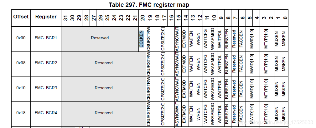
由于一个32位的数据占用地址为4个地址。所以有以下对应关系:
BTCR[0]——FMC_BCR1
BTCR[2]——FMC_BCR2
BTCR[4]——FMC_BCR3
BTCR[6]——FMC_BCR4
所以
#define FMC_NORSRAM_BANK1                       0x00000000U
#define FMC_NORSRAM_BANK2                       0x00000002U
#define FMC_NORSRAM_BANK3                       0x00000004U
#define FMC_NORSRAM_BANK4                       0x00000006U
HAL_SRAM_MspInit
void HAL_SRAM_MspInit(SRAM_HandleTypeDef *hsram)
{
    GPIO_InitTypeDef GPIO_Initure;

    __HAL_RCC_FMC_CLK_ENABLE();   //使能FMC时钟
    __HAL_RCC_GPIOD_CLK_ENABLE(); //使能GPIOD时钟
    __HAL_RCC_GPIOE_CLK_ENABLE(); //使能GPIOE时钟

    //初始化PD0,1,4,5,7,8,9,10,13,14,15
    GPIO_Initure.Pin = GPIO_PIN_0 | GPIO_PIN_1 | GPIO_PIN_4 | GPIO_PIN_5 | GPIO_PIN_7 | GPIO_PIN_8 |
                       GPIO_PIN_9 | GPIO_PIN_10 | GPIO_PIN_13 | GPIO_PIN_14 | GPIO_PIN_15;
    GPIO_Initure.Mode = GPIO_MODE_AF_PP;    //推挽复用
    GPIO_Initure.Pull = GPIO_PULLUP;        //上拉
    GPIO_Initure.Speed = GPIO_SPEED_HIGH;   //高速
    GPIO_Initure.Alternate = GPIO_AF12_FMC; //复用为FMC
    HAL_GPIO_Init(GPIOD, &GPIO_Initure);    //初始化

    //初始化PE7,8,9,10,11,12,13,14,15
    GPIO_Initure.Pin = GPIO_PIN_7 | GPIO_PIN_8 | GPIO_PIN_9 | GPIO_PIN_10 | GPIO_PIN_11 |
                       GPIO_PIN_12 | GPIO_PIN_13 | GPIO_PIN_14 | GPIO_PIN_15;
    HAL_GPIO_Init(GPIOE, &GPIO_Initure);
}
此函数是关于SRAM使用底层管脚的初始化。可以对应下表:

FMC_NORSRAM_Init
/**
  * @brief  Initialize the FMC_NORSRAM device according to the specified
  *         control parameters in the FMC_NORSRAM_InitTypeDef
  * @param  Device Pointer to NORSRAM device instance
  * @param  Init Pointer to NORSRAM Initialization structure
  * @retval HAL status
  */
HAL_StatusTypeDef FMC_NORSRAM_Init(FMC_NORSRAM_TypeDef *Device, FMC_NORSRAM_InitTypeDef *Init)
{
    /* 1.检测参数 */
    uint32_t tmpr = 0U;

    /* Check the parameters */
    assert_param(IS_FMC_NORSRAM_DEVICE(Device));
    assert_param(IS_FMC_NORSRAM_BANK(Init->NSBank));
    assert_param(IS_FMC_MUX(Init->DataAddressMux));
    assert_param(IS_FMC_MEMORY(Init->MemoryType));
    assert_param(IS_FMC_NORSRAM_MEMORY_WIDTH(Init->MemoryDataWidth));
    assert_param(IS_FMC_BURSTMODE(Init->BurstAccessMode));
    assert_param(IS_FMC_WAIT_POLARITY(Init->WaitSignalPolarity));
#if defined(STM32F427xx) || defined(STM32F437xx) || defined(STM32F429xx) || defined(STM32F439xx)
    assert_param(IS_FMC_WRAP_MODE(Init->WrapMode));
#endif /* STM32F427xx || STM32F437xx || STM32F429xx || STM32F439xx */
    assert_param(IS_FMC_WAIT_SIGNAL_ACTIVE(Init->WaitSignalActive));
    assert_param(IS_FMC_WRITE_OPERATION(Init->WriteOperation));
    assert_param(IS_FMC_WAITE_SIGNAL(Init->WaitSignal));
    assert_param(IS_FMC_EXTENDED_MODE(Init->ExtendedMode));
    assert_param(IS_FMC_ASYNWAIT(Init->AsynchronousWait));
    assert_param(IS_FMC_WRITE_BURST(Init->WriteBurst));
    assert_param(IS_FMC_CONTINOUS_CLOCK(Init->ContinuousClock));
    assert_param(IS_FMC_PAGESIZE(Init->PageSize));
#if defined(STM32F446xx) || defined(STM32F469xx) || defined(STM32F479xx)
    assert_param(IS_FMC_WRITE_FIFO(Init->WriteFifo));
#endif /* STM32F446xx || STM32F469xx || STM32F479xx */

    /* 2.写入寄存器 */
    /* Get the BTCR register value */
    tmpr = Device->BTCR[Init->NSBank];

#if defined(STM32F427xx) || defined(STM32F437xx) || defined(STM32F429xx) || defined(STM32F439xx)
    /* Clear MBKEN, MUXEN, MTYP, MWID, FACCEN, BURSTEN, WAITPOL, WRAPMOD, WAITCFG, WREN,
           WAITEN, EXTMOD, ASYNCWAIT, CPSIZE, CBURSTRW and CCLKEN bits */
    tmpr &= ((uint32_t) ~(FMC_BCR1_MBKEN | FMC_BCR1_MUXEN | FMC_BCR1_MTYP |
                          FMC_BCR1_MWID | FMC_BCR1_FACCEN | FMC_BCR1_BURSTEN |
                          FMC_BCR1_WAITPOL | FMC_BCR1_WRAPMOD | FMC_BCR1_WAITCFG |
                          FMC_BCR1_WREN | FMC_BCR1_WAITEN | FMC_BCR1_EXTMOD |
                          FMC_BCR1_ASYNCWAIT | FMC_BCR1_CPSIZE | FMC_BCR1_CBURSTRW |
                          FMC_BCR1_CCLKEN));

    /* Set NORSRAM device control parameters */
    tmpr |= (uint32_t)(Init->DataAddressMux |
                       Init->MemoryType |
                       Init->MemoryDataWidth |
                       Init->BurstAccessMode |
                       Init->WaitSignalPolarity |
                       Init->WrapMode |
                       Init->WaitSignalActive |
                       Init->WriteOperation |
                       Init->WaitSignal |
                       Init->ExtendedMode |
                       Init->AsynchronousWait |
                       Init->PageSize |
                       Init->WriteBurst |
                       Init->ContinuousClock);
#else  /* defined(STM32F446xx) || defined(STM32F469xx) || defined(STM32F479xx) */
    /* Clear MBKEN, MUXEN, MTYP, MWID, FACCEN, BURSTEN, WAITPOL, CPSIZE, WAITCFG, WREN,
           WAITEN, EXTMOD, ASYNCWAIT, CBURSTRW, CCLKEN and WFDIS bits */
    tmpr &= ((uint32_t) ~(FMC_BCR1_MBKEN | FMC_BCR1_MUXEN | FMC_BCR1_MTYP |
                          FMC_BCR1_MWID | FMC_BCR1_FACCEN | FMC_BCR1_BURSTEN |
                          FMC_BCR1_WAITPOL | FMC_BCR1_WAITCFG | FMC_BCR1_CPSIZE |
                          FMC_BCR1_WREN | FMC_BCR1_WAITEN | FMC_BCR1_EXTMOD |
                          FMC_BCR1_ASYNCWAIT | FMC_BCR1_CBURSTRW | FMC_BCR1_CCLKEN |
                          FMC_BCR1_WFDIS));

    /* Set NORSRAM device control parameters */
    tmpr |= (uint32_t)(Init->DataAddressMux |
                       Init->MemoryType |
                       Init->MemoryDataWidth |
                       Init->BurstAccessMode |
                       Init->WaitSignalPolarity |
                       Init->WaitSignalActive |
                       Init->WriteOperation |
                       Init->WaitSignal |
                       Init->ExtendedMode |
                       Init->AsynchronousWait |
                       Init->WriteBurst |
                       Init->ContinuousClock |
                       Init->PageSize |
                       Init->WriteFifo);
#endif /*  defined(STM32F427xx) || defined(STM32F437xx) || defined(STM32F429xx) || defined(STM32F439xx) */

    if (Init->MemoryType == FMC_MEMORY_TYPE_NOR)
    {
        tmpr |= (uint32_t)FMC_NORSRAM_FLASH_ACCESS_ENABLE;
    }

    Device->BTCR[Init->NSBank] = tmpr;

    /* Configure synchronous mode when Continuous clock is enabled for bank2..4 */
    if ((Init->ContinuousClock == FMC_CONTINUOUS_CLOCK_SYNC_ASYNC) && (Init->NSBank != FMC_NORSRAM_BANK1))
    {
        Device->BTCR[FMC_NORSRAM_BANK1] |= (uint32_t)(Init->ContinuousClock);
    }

#if defined(STM32F446xx) || defined(STM32F469xx) || defined(STM32F479xx)
    if (Init->NSBank != FMC_NORSRAM_BANK1)
    {
        Device->BTCR[FMC_NORSRAM_BANK1] |= (uint32_t)(Init->WriteFifo);
    }
#endif /* STM32F446xx || STM32F469xx || STM32F479xx */

    return HAL_OK;
}
该函数比较容易理解,即将结构体FMC_NORSRAM_InitTypeDef中的成员变量的值,写入到寄存器中。在HAL库中,写入寄存器的经典步骤为:
- 将原有的寄存器的值存入临时变量中。
- 将需要写入的值对应临时变量的位数清零。
- 将值写入临时变量。
- 将临时变量写入到寄存器中。
其中,若寄存器类型是NORFLASH时,将使能对应的位,通过以下语句。
    if (Init->MemoryType == FMC_MEMORY_TYPE_NOR)
    {
        tmpr |= (uint32_t)FMC_NORSRAM_FLASH_ACCESS_ENABLE;
    }
若SRAM使用的并非BANK1而要连续同步时钟时,则需要将BANK1的对应位置位。这是因为只有BANK1对应位管理整个空间,通过以下语句实现:
    if ((Init->ContinuousClock == FMC_CONTINUOUS_CLOCK_SYNC_ASYNC) && (Init->NSBank != FMC_NORSRAM_BANK1))
    {
        Device->BTCR[FMC_NORSRAM_BANK1] |= (uint32_t)(Init->ContinuousClock);
    }
获取寄存器原有值通过以语句实现:
tmpr = Device->BTCR[Init->NSBank];
之所以,这种方式,在上文已经分析,此处不再介绍。
后文中的FMC_NORSRAM_Timing_Init和FMC_NORSRAM_Extended_Timing_Init 与上文内容基本一致,不再详细介绍。
应用程序
应用程序中,最重要的就是写入字符串的实现LCD_ShowString。由于该函数由正点原子实现,本文不再粘贴其源代码。其大致思想是调用LCD_ShowChar函数实现。在LCD_ShowChar函数中,将ASCII编码转化为LCD对应的编码。最后将编码处理为LCD每个点,调用LCD_Fast_DrawPoint()函数将点的颜色与位置输出。
这里考虑到不同屏幕的通用性,在显示每次LCD点时,都设置一次打点的位置。这在35510是非必要的。在下面博客实现的工程中,将会对此进行改造。


 701
701


 被折叠的 条评论
为什么被折叠?
被折叠的 条评论
为什么被折叠?
 到【灌水乐园】发言


