FPGA内部资源(一)DSP48E1

一、 实验过程中发现的问题

使用ISE进行项目的实现时出现以下错误。
在这里插入图片描述
在这里插入图片描述
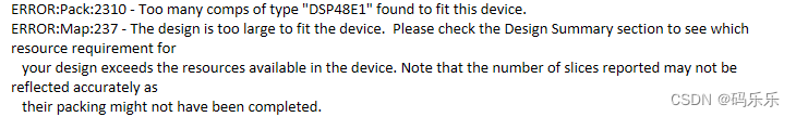
意思很简单,就是使用DSP48E1的数量超出限制,因为没有接触过DSP48E1,所以尝试了很多错误的方法后,我找到项目下的.mrp文件,里面有一行显示 Number of DSP48E1s: 496 out of 480 103%,也就是说我使用的 XC6V1x130t 型号FPGA只有480个DSP48E1,但是我使用了496个。
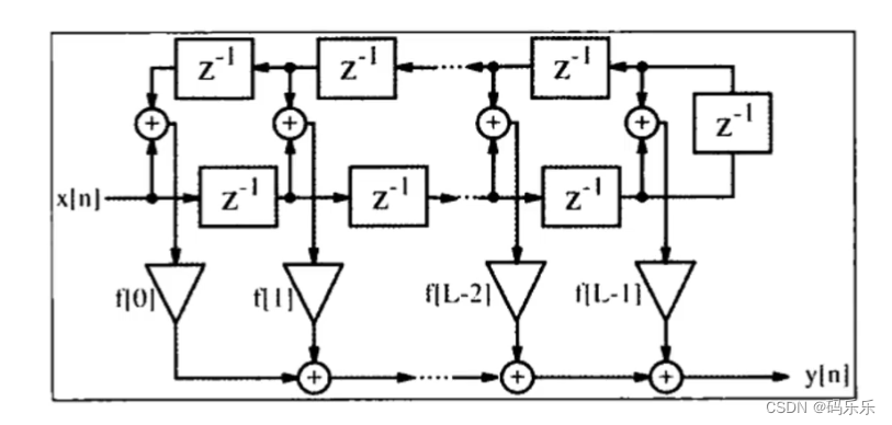
我的项目中用到了4个fir滤波器,都是160阶的,而且其中两个系数对称,另外两个系数不对称,我在代码中尝试添加其中的某个滤波器,发现系数对称的滤波器会占用80个DSP48E1,系数不对称的fir滤波器会占用160个DSP48E1,并且结合查阅到的资料,DSP48E1主要是用来做乘法器使用的,这就非常合理了,对称的系数可以使用如下结构实现,确实节省一半的乘法器。实际上,fir滤波器的底层实现就是通过多个DSP48E1级联实现的。可以参考
在这里插入图片描述

于是,我适当减少了fir滤波器的系数个数,最终可以成功实现。

二、学习DSP48E1

DSP48E1结构图
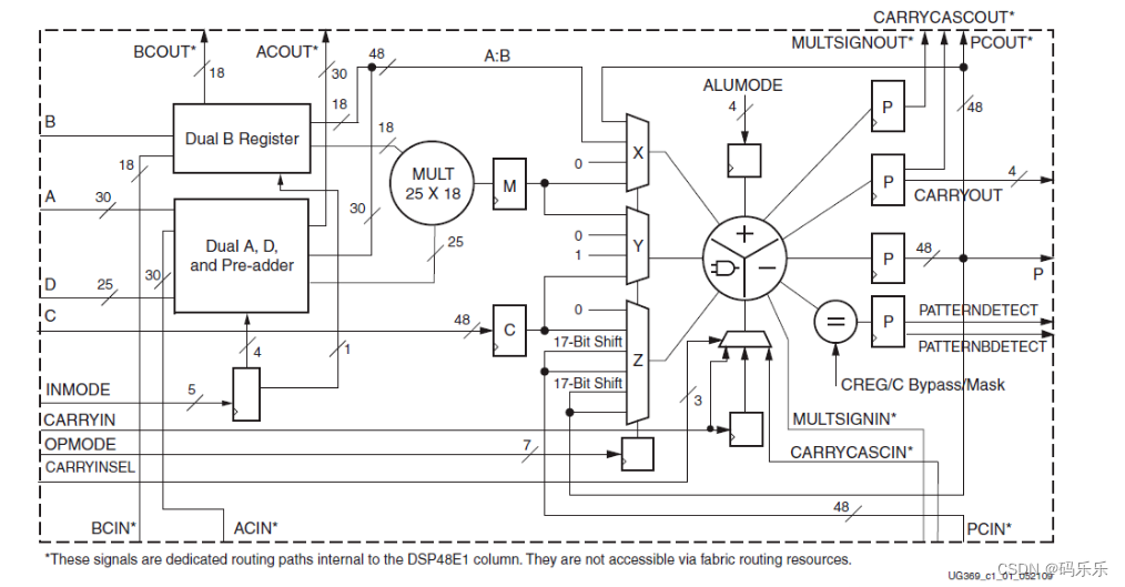
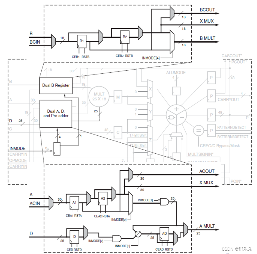
图中带*号的信号是级联专用信号,只在级联时使用,用户逻辑访问不了。我们只需要关注A、B、C、D、P、INMODE、OPMODE、ALUMODE这几个信号的使用即可。
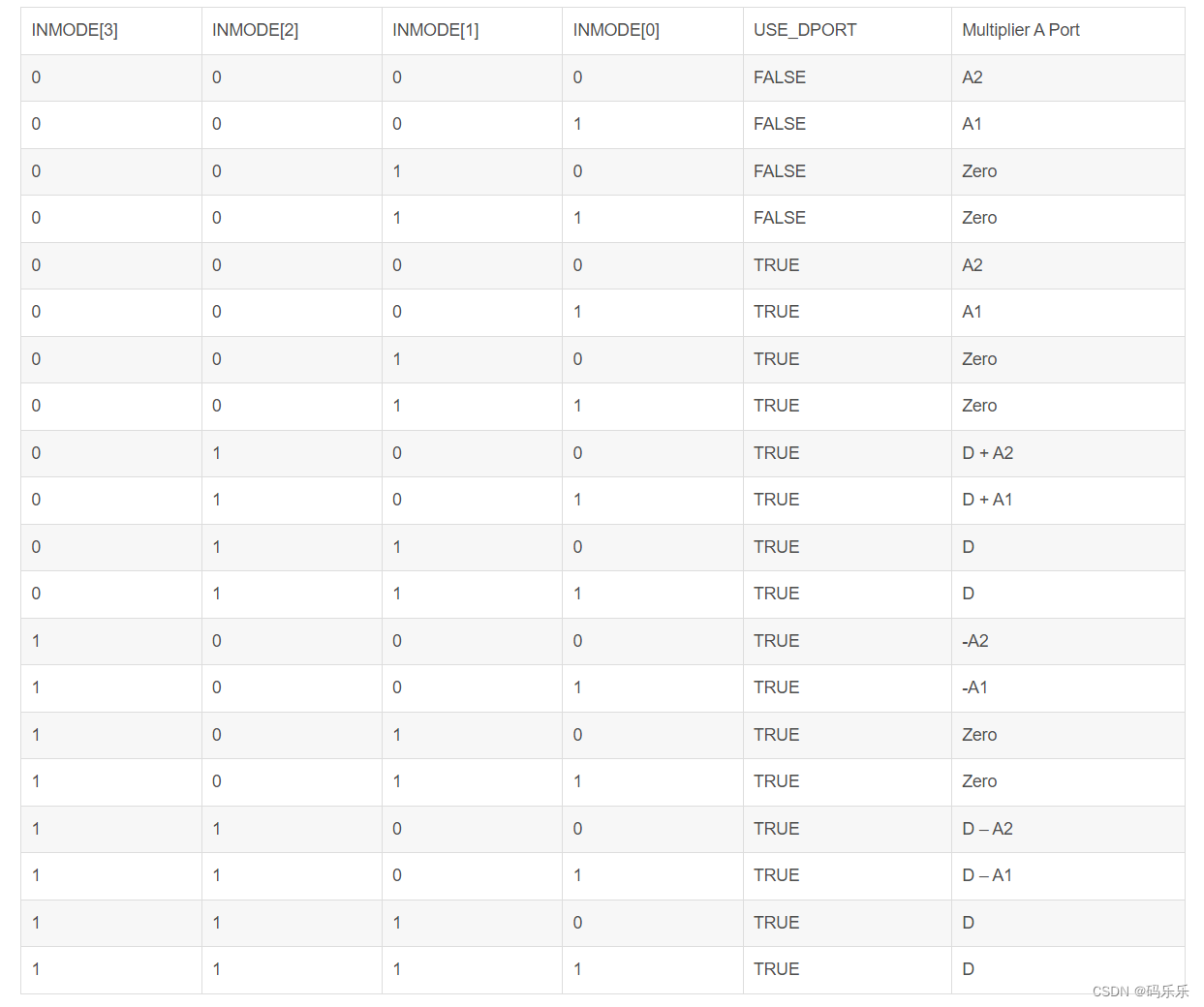
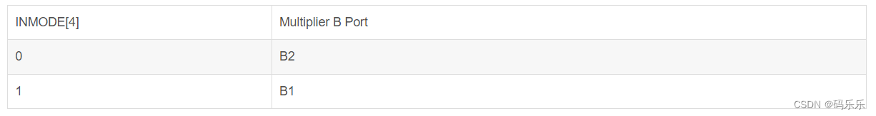
INMODE

在这里插入图片描述
上图主要反映了INMODE与打拍寄存器的关系,可以用下面两个表概括,INMODE一般配置为7’b0000101,做乘法器使用。
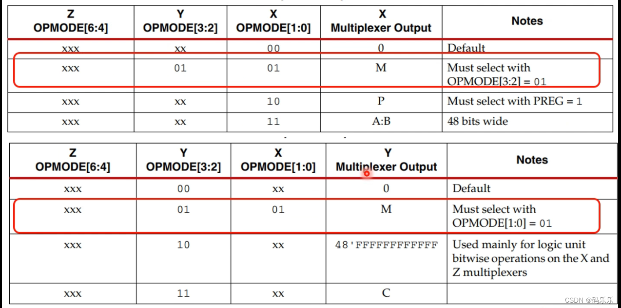
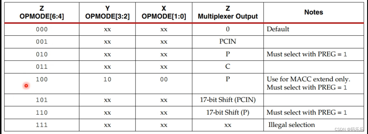
在这里插入图片描述
在这里插入图片描述

OPMODE

X、Y、Z输出与OPMODE的关系如下表所示。
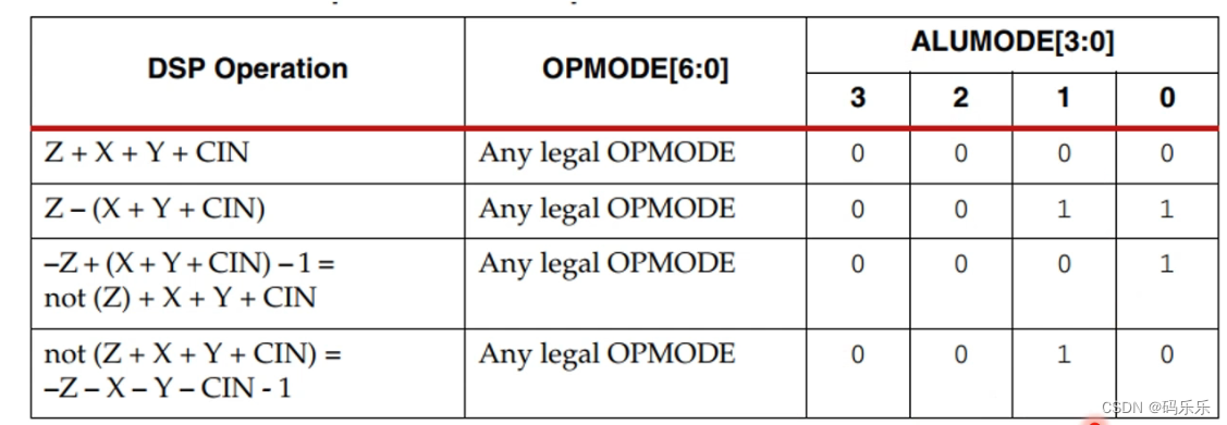
在这里插入图片描述
在这里插入图片描述

ALUMODE

最终P端口输出与ALUMODE的关系如下所示,其中的CIN就是48位输入信号C。
在这里插入图片描述

例程

`timescale 1ns / 1ps
//
// Company: 
// Engineer: 
// 
// Create Date: 2024/06/19 16:58:05
// Design Name: 
// Module Name: tb_DSP48E1
// Project Name: 
// Target Devices: 
// Tool Versions: 
// Description: 
// 
// Dependencies: 
// 
// Revision:
// Revision 0.01 - File Created
// Additional Comments:
// 
//


module tb_DSP48E1();

    reg R_clk;
    reg R_reset;
    reg[29:0] R_A;
    reg[24:0] R_D;
    reg[47:0] R_C;
    reg[17:0] R_B;

    wire[47:0] W_P;
    wire[47:0] W_PCIN;

    reg[4:0] INMODE;
    reg[6:0] OPMODE;
    reg[3:0] ALUMODE;

    reg[3:0] R_num;

    initial begin
        R_clk = 1'b0;
        R_reset = 1'b1;
        R_A = 30'd100;
        R_B = 18'd2;
        R_C = 48'd2000;
        R_D = 25'd200;
        R_num = 4'd0;
        OPMODE = 7'b0000101;        // X-M  Y-M  Z-0
        INMODE = 5'b00101;          // (D+A1) * B2      这三个输出刚好对齐,第三拍得到运算结果
        ALUMODE = 4'b0000;          // X+Y+Z+C
        #100 R_reset = 1'b0;
    end

    always#5 R_clk = ~R_clk;

    always @(posedge R_clk) begin
        if(R_reset)begin
            R_A <= 30'd100;
            R_B <= 18'd2;
            R_C <= 48'd2000;
            R_D <= 25'd200;
            R_num <= 4'd0;
        end
        else if(R_num < 9)begin
            R_num <= R_num + 1'b1;
            R_A <= R_A + 1'b1;
            R_B <= R_B + 1'b1;
            R_C <= R_C + 1'b1;
            R_D <= R_D + 1'b1;
        end
        else begin
            OPMODE <= 7'b0110101;   // X-M  Y-M  Z-C
            R_A <= R_A + 1'b1;
            R_B <= R_B + 1'b1;
            R_C <= R_C + 1'b1;
            R_D <= R_D + 1'b1;
        end
    end

    DSP48E1 #(
      // Feature Control Attributes: Data Path Selection
      .A_INPUT("DIRECT"),               // Selects A input source, "DIRECT" (A port) or "CASCADE" (ACIN port)
      .B_INPUT("DIRECT"),               // Selects B input source, "DIRECT" (B port) or "CASCADE" (BCIN port)
      .USE_DPORT("TRUE"),              // Select D port usage (TRUE or FALSE)
      .USE_MULT("MULTIPLY"),            // Select multiplier usage ("MULTIPLY", "DYNAMIC", or "NONE")
      .USE_SIMD("ONE48"),               // SIMD selection ("ONE48", "TWO24", "FOUR12")
      // Pattern Detector Attributes: Pattern Detection Configuration
      .AUTORESET_PATDET("NO_RESET"),    // "NO_RESET", "RESET_MATCH", "RESET_NOT_MATCH" 
      .MASK(48'h3fffffffffff),          // 48-bit mask value for pattern detect (1=ignore)
      .PATTERN(48'h000000000000),       // 48-bit pattern match for pattern detect
      .SEL_MASK("MASK"),                // "C", "MASK", "ROUNDING_MODE1", "ROUNDING_MODE2" 
      .SEL_PATTERN("PATTERN"),          // Select pattern value ("PATTERN" or "C")
      .USE_PATTERN_DETECT("NO_PATDET"), // Enable pattern detect ("PATDET" or "NO_PATDET")
      // Register Control Attributes: Pipeline Register Configuration
      .ACASCREG(1),                     // Number of pipeline stages between A/ACIN and ACOUT (0, 1 or 2)
      .ADREG(1),                        // Number of pipeline stages for pre-adder (0 or 1)
      .ALUMODEREG(1),                   // Number of pipeline stages for ALUMODE (0 or 1)
      .AREG(1),                         // Number of pipeline stages for A (0, 1 or 2)
      .BCASCREG(1),                     // Number of pipeline stages between B/BCIN and BCOUT (0, 1 or 2)
      .BREG(2),                         // Number of pipeline stages for B (0, 1 or 2)                          这里要用到B2,所以要置为2
      .CARRYINREG(1),                   // Number of pipeline stages for CARRYIN (0 or 1)
      .CARRYINSELREG(1),                // Number of pipeline stages for CARRYINSEL (0 or 1)
      .CREG(1),                         // Number of pipeline stages for C (0 or 1)
      .DREG(1),                         // Number of pipeline stages for D (0 or 1)
      .INMODEREG(1),                    // Number of pipeline stages for INMODE (0 or 1)
      .MREG(1),                         // Number of multiplier pipeline stages (0 or 1)
      .OPMODEREG(1),                    // Number of pipeline stages for OPMODE (0 or 1)
      .PREG(1)                          // Number of pipeline stages for P (0 or 1)
   )
   DSP48E1_inst (
      // Cascade: 30-bit (each) output: Cascade Ports
      .ACOUT(),                   // 30-bit output: A port cascade output
      .BCOUT(),                   // 18-bit output: B port cascade output
      .CARRYCASCOUT(),     // 1-bit output: Cascade carry output
      .MULTSIGNOUT(),       // 1-bit output: Multiplier sign cascade output
      .PCOUT(),                   // 48-bit output: Cascade output
      // Control: 1-bit (each) output: Control Inputs/Status Bits
      .OVERFLOW(),             // 1-bit output: Overflow in add/acc output
      .PATTERNBDETECT(), // 1-bit output: Pattern bar detect output
      .PATTERNDETECT(),   // 1-bit output: Pattern detect output
      .UNDERFLOW(),           // 1-bit output: Underflow in add/acc output
      // Data: 4-bit (each) output: Data Ports
      .CARRYOUT(),             // 4-bit output: Carry output
      .P(W_P),                           // 48-bit output: Primary data output
      // Cascade: 30-bit (each) input: Cascade Ports
      .ACIN(1'b0),                     // 30-bit input: A cascade data input
      .BCIN(1'b0),                     // 18-bit input: B cascade input
      .CARRYCASCIN(1'b1),       // 1-bit input: Cascade carry input
      .MULTSIGNIN(1'b1),         // 1-bit input: Multiplier sign input
      .PCIN(W_PCIN),                     // 48-bit input: P cascade input
      // Control: 4-bit (each) input: Control Inputs/Status Bits
      .ALUMODE(ALUMODE),               // 4-bit input: ALU control input
      .CARRYINSEL(3'd0),         // 3-bit input: Carry select input
      .CLK(R_clk),                       // 1-bit input: Clock input
      .INMODE(INMODE),                 // 5-bit input: INMODE control input
      .OPMODE(OPMODE),                 // 7-bit input: Operation mode input
      // Data: 30-bit (each) input: Data Ports
      .A(R_A),                           // 30-bit input: A data input
      .B(R_B),                           // 18-bit input: B data input
      .C(R_C),                           // 48-bit input: C data input
      .CARRYIN(1'b0),               // 1-bit input: Carry input signal
      .D(R_D),                           // 25-bit input: D data input
      // Reset/Clock Enable: 1-bit (each) input: Reset/Clock Enable Inputs
      .CEA1(1'b1),                     // 1-bit input: Clock enable input for 1st stage AREG
      .CEA2(1'b1),                     // 1-bit input: Clock enable input for 2nd stage AREG
      .CEAD(1'b1),                     // 1-bit input: Clock enable input for ADREG
      .CEALUMODE(1'b1),           // 1-bit input: Clock enable input for ALUMODE
      .CEB1(1'b1),                     // 1-bit input: Clock enable input for 1st stage BREG
      .CEB2(1'b1),                     // 1-bit input: Clock enable input for 2nd stage BREG
      .CEC(1'b1),                       // 1-bit input: Clock enable input for CREG
      .CECARRYIN(1'b1),           // 1-bit input: Clock enable input for CARRYINREG
      .CECTRL(1'b1),                 // 1-bit input: Clock enable input for OPMODEREG and CARRYINSELREG
      .CED(1'b1),                       // 1-bit input: Clock enable input for DREG
      .CEINMODE(1'b1),             // 1-bit input: Clock enable input for INMODEREG
      .CEM(1'b1),                       // 1-bit input: Clock enable input for MREG
      .CEP(1'b1),                       // 1-bit input: Clock enable input for PREG

      .RSTA(R_reset),                     // 1-bit input: Reset input for AREG
      .RSTALLCARRYIN(R_reset),   // 1-bit input: Reset input for CARRYINREG
      .RSTALUMODE(R_reset),         // 1-bit input: Reset input for ALUMODEREG
      .RSTB(R_reset),                     // 1-bit input: Reset input for BREG
      .RSTC(R_reset),                     // 1-bit input: Reset input for CREG
      .RSTCTRL(R_reset),               // 1-bit input: Reset input for OPMODEREG and CARRYINSELREG
      .RSTD(R_reset),                     // 1-bit input: Reset input for DREG and ADREG
      .RSTINMODE(R_reset),           // 1-bit input: Reset input for INMODEREG
      .RSTM(R_reset),                     // 1-bit input: Reset input for MREG
      .RSTP(R_reset)                      // 1-bit input: Reset input for PREG
   );
endmodule

运行结果如下图所示。
在这里插入图片描述
从DSP48E1结构图也能看出,最终输出结果P会在A、B、C、D输入的第四拍输出,并且C与A、B、D相差两拍,OPMODE也会延迟一拍配置进去,所以改变OPMODE之后,结果会是5170 = (108+208)* 10 + 2010,输出结果符合预期。
按照代码中的配置,X = M,Y=M,理论上加起来应该是2M,但实际就是M,这里应该是乘法器分两部分进行乘法操作,所以最后X+Y = M。

使用DSP48E1实现fir的卷积功能

主程序如下

`timescale 1ns / 1ps
//
// Company: 
// Engineer: 
// 
// Create Date: 2024/06/22 11:15:16
// Design Name: 
// Module Name: pck_fir
// Project Name: 
// Target Devices: 
// Tool Versions: 
// Description: 
// 
// Dependencies: 
// 
// Revision:
// Revision 0.01 - File Created
// Additional Comments:
// 
//

// 使用dsp48e1实现fir滤波器
// 先串行输入滤波器系数,假设 x = [1,2...11]
// 再串行输入信号,假设 t = [31,32...1000]
// 最后得到结果为 y = conv(x,t)
module pck_fir # (
    parameter C_COE_WIDTH = 16,
    parameter C_INPUT_WIDTH = 16,
    parameter C_OUTPUT_WIDTH = 48,
    parameter C_COE_NUM = 11
)
(
    input I_clk,
    input I_rst,
    input I_coe_param_vd,
    input[C_COE_WIDTH-1:0] I_coe_param,
    input I_data_vd,
    input[C_INPUT_WIDTH-1:0] I_data,
    output[C_OUTPUT_WIDTH-1:0] O_data
);

localparam C_A_WIDTH = 30;
localparam C_B_WIDTH = 18;
localparam C_C_WIDTH = 48;
localparam C_D_WIDTH = 25;
localparam C_P_WIDTH = 48;

reg[C_B_WIDTH-1:0] R_coe_params[C_COE_NUM-1:0];
reg[C_A_WIDTH-1:0] R_data;

wire[47:0] W_cin;
wire[24:0] W_din;
wire[47:0] W_pin;
wire[47:0] W_pout[C_COE_NUM-1:0];

assign W_cin = 48'd0;
assign W_din = 25'd0;
assign W_pin = 48'd0;

always @(posedge I_clk or negedge I_rst) begin
    if(~I_rst)begin
        R_data <= 'd0;
    end
    else if(I_data_vd)begin
        R_data[C_INPUT_WIDTH-1:0] <= I_data;
    end
    else
        R_data <= 0;
end

genvar i;
generate
    for(i = 0;i < C_COE_NUM;i = i + 1)
    begin
        always @(posedge I_clk or negedge I_rst) begin
            if(~I_rst)begin
                R_coe_params[i] <= 'd0;
            end
            else begin
                if(I_coe_param_vd)begin
                    if(i == 0)
                        R_coe_params[i][C_COE_WIDTH-1:0] <= I_coe_param;
                    else
                        R_coe_params[i] <= R_coe_params[i-1]; 
                end
                else
                    R_coe_params[i] <= R_coe_params[i];
            end
        end
    end
endgenerate

pck_dsp48e1 pck_1(
    .I_clk(I_clk),
    .I_rst(~I_rst),
    .A(R_data),
    .B(R_coe_params[0]),
    .C(W_cin),
    .D(W_din),
    .PCIN(W_pin),
    .P(),
    .PCOUT(W_pout[0])
);

genvar k;
generate
    for(k = 1;k < C_COE_NUM;k = k + 1)
    begin:dsp_gen
        pck_dsp48e1 #(
            .C_OPMODE(7'b0010101)
        ) pck_n(
            .I_clk(I_clk),
            .I_rst(~I_rst),
            .A(R_data),
            .B(R_coe_params[k]),
            .C(W_cin),
            .D(W_din),
            .PCIN(W_pout[k-1]),
            .P(),
            .PCOUT(W_pout[k])
        );
    end
endgenerate

assign O_data = W_pout[C_COE_NUM-1];

endmodule

由于DSP48E1参数较多,可以进行适当封装,封装后如下。

`timescale 1ns / 1ps
//
// Company: 
// Engineer: 
// 
// Create Date: 2024/06/22 10:45:31
// Design Name: 
// Module Name: pck_dsp48e1
// Project Name: 
// Target Devices: 
// Tool Versions: 
// Description: 
// 
// Dependencies: 
// 
// Revision:
// Revision 0.01 - File Created
// Additional Comments:
// 
//


module pck_dsp48e1 # (
    parameter C_ALUMODE = 4'b0000,
    parameter C_INMODE = 5'b00101,
    parameter C_OPMODE = 7'b0000101
)
(
    input I_clk,
    input I_rst,
    input[29:0] A,
    input[17:0] B,
    input[47:0] C,
    input[24:0] D,
    input[47:0] PCIN,
    output[47:0] P,
    output[47:0] PCOUT
);

    DSP48E1 #(
      // Feature Control Attributes: Data Path Selection
      .A_INPUT("DIRECT"),               // Selects A input source, "DIRECT" (A port) or "CASCADE" (ACIN port)
      .B_INPUT("DIRECT"),               // Selects B input source, "DIRECT" (B port) or "CASCADE" (BCIN port)
      .USE_DPORT("TRUE"),              // Select D port usage (TRUE or FALSE)
      .USE_MULT("MULTIPLY"),            // Select multiplier usage ("MULTIPLY", "DYNAMIC", or "NONE")
      .USE_SIMD("ONE48"),               // SIMD selection ("ONE48", "TWO24", "FOUR12")
      // Pattern Detector Attributes: Pattern Detection Configuration
      .AUTORESET_PATDET("NO_RESET"),    // "NO_RESET", "RESET_MATCH", "RESET_NOT_MATCH" 
      .MASK(48'h3fffffffffff),          // 48-bit mask value for pattern detect (1=ignore)
      .PATTERN(48'h000000000000),       // 48-bit pattern match for pattern detect
      .SEL_MASK("MASK"),                // "C", "MASK", "ROUNDING_MODE1", "ROUNDING_MODE2" 
      .SEL_PATTERN("PATTERN"),          // Select pattern value ("PATTERN" or "C")
      .USE_PATTERN_DETECT("NO_PATDET"), // Enable pattern detect ("PATDET" or "NO_PATDET")
      // Register Control Attributes: Pipeline Register Configuration
      .ACASCREG(1),                     // Number of pipeline stages between A/ACIN and ACOUT (0, 1 or 2)
      .ADREG(1),                        // Number of pipeline stages for pre-adder (0 or 1)
      .ALUMODEREG(1),                   // Number of pipeline stages for ALUMODE (0 or 1)
      .AREG(1),                         // Number of pipeline stages for A (0, 1 or 2)
      .BCASCREG(1),                     // Number of pipeline stages between B/BCIN and BCOUT (0, 1 or 2)
      .BREG(2),                         // Number of pipeline stages for B (0, 1 or 2)                          这里要用到B2,所以要置为2
      .CARRYINREG(1),                   // Number of pipeline stages for CARRYIN (0 or 1)
      .CARRYINSELREG(1),                // Number of pipeline stages for CARRYINSEL (0 or 1)
      .CREG(1),                         // Number of pipeline stages for C (0 or 1)
      .DREG(1),                         // Number of pipeline stages for D (0 or 1)
      .INMODEREG(1),                    // Number of pipeline stages for INMODE (0 or 1)
      .MREG(1),                         // Number of multiplier pipeline stages (0 or 1)
      .OPMODEREG(1),                    // Number of pipeline stages for OPMODE (0 or 1)
      .PREG(1)                          // Number of pipeline stages for P (0 or 1)
   )
   DSP48E1_inst (
      // Cascade: 30-bit (each) output: Cascade Ports
      .ACOUT(),                   // 30-bit output: A port cascade output
      .BCOUT(),                   // 18-bit output: B port cascade output
      .CARRYCASCOUT(),     // 1-bit output: Cascade carry output
      .MULTSIGNOUT(),       // 1-bit output: Multiplier sign cascade output
      .PCOUT(PCOUT),                   // 48-bit output: Cascade output
      // Control: 1-bit (each) output: Control Inputs/Status Bits
      .OVERFLOW(),             // 1-bit output: Overflow in add/acc output
      .PATTERNBDETECT(), // 1-bit output: Pattern bar detect output
      .PATTERNDETECT(),   // 1-bit output: Pattern detect output
      .UNDERFLOW(),           // 1-bit output: Underflow in add/acc output
      // Data: 4-bit (each) output: Data Ports
      .CARRYOUT(),             // 4-bit output: Carry output
      .P(P),                           // 48-bit output: Primary data output
      // Cascade: 30-bit (each) input: Cascade Ports
      .ACIN(1'b0),                     // 30-bit input: A cascade data input
      .BCIN(1'b0),                     // 18-bit input: B cascade input
      .CARRYCASCIN(1'b1),       // 1-bit input: Cascade carry input
      .MULTSIGNIN(1'b1),         // 1-bit input: Multiplier sign input
      .PCIN(PCIN),                     // 48-bit input: P cascade input
      // Control: 4-bit (each) input: Control Inputs/Status Bits
      .ALUMODE(C_ALUMODE),               // 4-bit input: ALU control input
      .CARRYINSEL(3'd0),         // 3-bit input: Carry select input
      .CLK(I_clk),                       // 1-bit input: Clock input
      .INMODE(C_INMODE),                 // 5-bit input: INMODE control input
      .OPMODE(C_OPMODE),                 // 7-bit input: Operation mode input
      // Data: 30-bit (each) input: Data Ports
      .A(A),                           // 30-bit input: A data input
      .B(B),                           // 18-bit input: B data input
      .C(C),                           // 48-bit input: C data input
      .CARRYIN(1'b0),               // 1-bit input: Carry input signal
      .D(D),                           // 25-bit input: D data input
      // Reset/Clock Enable: 1-bit (each) input: Reset/Clock Enable Inputs
      .CEA1(1'b1),                     // 1-bit input: Clock enable input for 1st stage AREG
      .CEA2(1'b1),                     // 1-bit input: Clock enable input for 2nd stage AREG
      .CEAD(1'b1),                     // 1-bit input: Clock enable input for ADREG
      .CEALUMODE(1'b1),           // 1-bit input: Clock enable input for ALUMODE
      .CEB1(1'b1),                     // 1-bit input: Clock enable input for 1st stage BREG
      .CEB2(1'b1),                     // 1-bit input: Clock enable input for 2nd stage BREG
      .CEC(1'b1),                       // 1-bit input: Clock enable input for CREG
      .CECARRYIN(1'b1),           // 1-bit input: Clock enable input for CARRYINREG
      .CECTRL(1'b1),                 // 1-bit input: Clock enable input for OPMODEREG and CARRYINSELREG
      .CED(1'b1),                       // 1-bit input: Clock enable input for DREG
      .CEINMODE(1'b1),             // 1-bit input: Clock enable input for INMODEREG
      .CEM(1'b1),                       // 1-bit input: Clock enable input for MREG
      .CEP(1'b1),                       // 1-bit input: Clock enable input for PREG

      .RSTA(I_rst),                     // 1-bit input: Reset input for AREG
      .RSTALLCARRYIN(I_rst),   // 1-bit input: Reset input for CARRYINREG
      .RSTALUMODE(I_rst),         // 1-bit input: Reset input for ALUMODEREG
      .RSTB(I_rst),                     // 1-bit input: Reset input for BREG
      .RSTC(I_rst),                     // 1-bit input: Reset input for CREG
      .RSTCTRL(I_rst),               // 1-bit input: Reset input for OPMODEREG and CARRYINSELREG
      .RSTD(I_rst),                     // 1-bit input: Reset input for DREG and ADREG
      .RSTINMODE(I_rst),           // 1-bit input: Reset input for INMODEREG
      .RSTM(I_rst),                     // 1-bit input: Reset input for MREG
      .RSTP(I_rst)                      // 1-bit input: Reset input for PREG
   );

endmodule

测试代码如下。

`timescale 1ns / 1ps
//
// Company: 
// Engineer: 
// 
// Create Date: 2024/06/22 15:35:29
// Design Name: 
// Module Name: tb_pck_fir
// Project Name: 
// Target Devices: 
// Tool Versions: 
// Description: 
// 
// Dependencies: 
// 
// Revision:
// Revision 0.01 - File Created
// Additional Comments:
// 
//


module tb_pck_fir();

    reg R_clk;
    reg R_data_vd;
    reg R_coe_data_vd;
    wire[15:0] W_data;
    wire[15:0] W_coe_data;
    reg R_rst;

    reg[15:0] R_cnt;

    wire[47:0] W_res;

    initial begin
        R_clk = 1'b0;
        R_rst = 1'b0;
        R_cnt = 5'd0;
        R_data_vd = 1'b0;
        R_coe_data_vd = 1'b0;

        #2000 R_rst = 1'b1;
    end

    always#5 R_clk = ~R_clk;

    always @(posedge R_clk) begin
        if(~R_rst)begin
            R_cnt <= 16'd0;
        end
        else if(R_cnt < 'd11)begin
            R_cnt <= R_cnt + 1;
            R_coe_data_vd <= 1'b1;
        end
        else if(R_cnt == 'd11)begin
            R_coe_data_vd <= 1'b0;
            R_cnt <= R_cnt + 1;
        end
        else if(R_cnt == 'd30)begin
            R_cnt <= R_cnt + 1;
            R_data_vd <= 1'b1;
        end
        else if(R_cnt > 'd1000)begin
            R_data_vd <= 1'b0;
            R_cnt <= R_cnt;
        end
        else
            R_cnt <= R_cnt + 1;
    end

    assign W_coe_data = R_cnt;
    assign W_data = R_cnt;

    pck_fir pf(
        .I_clk(R_clk),
        .I_rst(R_rst),
        .I_coe_param_vd(R_coe_data_vd),
        .I_coe_param(W_coe_data),
        .I_data_vd(R_data_vd),
        .I_data(W_data),
        .O_data(W_res)
    );

endmodule

仿真结果如下

在这里插入图片描述
在这里插入图片描述
结果正确,实现了[1,2…11] 卷积 [31,32…1001]

使用DSP48E1实现复数乘法

使用DSP48E1实现的复数乘法相对于传统方法可以减少一个乘法器,从而节省了内部资源。
主程序如下。

`timescale 1ns / 1ps
//
// Company: 
// Engineer: 
// 
// Create Date: 2024/06/22 20:02:25
// Design Name: 
// Module Name: Complex_Multiple
// Project Name: 
// Target Devices: 
// Tool Versions: 
// Description: 
// 
// Dependencies: 
// 
// Revision:
// Revision 0.01 - File Created
// Additional Comments:
// 
//

// (a+bj)*(c+dj) = (ac-bd)+(ad+bc)j = [(a+b)c - b(c+d)] + [(a+b)c + a(d-c)]

module Complex_Multiple(
    input I_clk,
    input I_rst_n,
    input[15:0] I_signal_I1,
    input[15:0] I_signal_Q1,
    input[15:0] I_signal_I2,
    input[15:0] I_signal_Q2,
    output[47:0] O_signal_I,
    output[47:0] O_signal_Q
    );

    localparam C_A_WIDTH = 30;
    localparam C_B_WIDTH = 18;
    localparam C_C_WIDTH = 48;
    localparam C_D_WIDTH = 25;
    localparam C_P_WIDTH = 48;

    wire[47:0] W_cin;
    wire[24:0] W_din;
    wire[47:0] W_pin;
    wire[47:0] W_p1,W_p2,W_p3;

    assign W_cin = 48'd0;
    assign W_din = 25'd0;
    assign W_pin = 48'd0;

    reg[C_A_WIDTH-1:0] R1_I1;
    reg[C_B_WIDTH-1:0] R1_I2;

    reg[C_D_WIDTH-1:0] R1_Q1;
    reg[C_B_WIDTH-1:0] R1_Q2;

    reg[C_A_WIDTH-1:0] R2_I1;
    reg[C_B_WIDTH-1:0] R2_I2;

    reg[C_D_WIDTH-1:0] R2_Q1;
    reg[C_A_WIDTH-1:0] R2_Q2;

    always @(posedge I_clk or negedge I_rst_n) begin
        if(~I_rst_n)begin
            R1_I1 <= 'd0;
            R1_I2 <= 'd0;
        end
        else begin
            R1_I1 <= I_signal_I1;
            R1_I2 <= I_signal_I1;
        end
    end

    always @(posedge I_clk or negedge I_rst_n) begin
        if(~I_rst_n)begin
            R1_Q1 <= 'd0;
            R1_Q2 <= 'd0;
        end
        else begin
            R1_Q1 <= I_signal_Q1;
            R1_Q2 <= I_signal_Q1;
        end
    end

    always @(posedge I_clk or negedge I_rst_n) begin
        if(~I_rst_n)begin
            R2_I1 <= 'd0;
            R2_I2 <= 'd0;
        end
        else begin
            R2_I1 <= I_signal_I2;
            R2_I2 <= I_signal_I2;
        end
    end

    always @(posedge I_clk or negedge I_rst_n) begin
        if(~I_rst_n)begin
            R2_Q1 <= 'd0;
            R2_Q2 <= 'd0;
        end
        else begin
            R2_Q1 <= I_signal_Q2;
            R2_Q2 <= I_signal_Q2;
        end
    end
    // (a+b)c
    pck_dsp48e1 pk1(
        .I_clk(I_clk),
        .I_rst(~I_rst_n),
        .A(R1_I1),
        .B(R2_I2),
        .C(W_cin),
        .D(R1_Q1),
        .PCIN(W_pin),
        .P(W_p1),
        .PCOUT()
    );

    // (c+d)b
    pck_dsp48e1 pk2(
        .I_clk(I_clk),
        .I_rst(~I_rst_n),
        .A(R2_I1),
        .B(R1_Q2),
        .C(W_cin),
        .D(R2_Q1),
        .PCIN(W_pin),
        .P(W_p2),
        .PCOUT()
    );

    // (d-c)a
    pck_dsp48e1 #(
        .C_INMODE(5'b01101)
    )pk3(
        .I_clk(I_clk),
        .I_rst(~I_rst_n),
        .A(R2_I1),
        .B(R1_I2),
        .C(W_cin),
        .D(R2_Q1),
        .PCIN(W_pin),
        .P(W_p3),
        .PCOUT()
    );

    assign O_signal_I = W_p1 - W_p2;
    assign O_signal_Q = W_p1 + W_p3;

endmodule

测试代码如下。

`timescale 1ns / 1ps
//
// Company: 
// Engineer: 
// 
// Create Date: 2024/06/23 13:51:50
// Design Name: 
// Module Name: tb_complex_multiple
// Project Name: 
// Target Devices: 
// Tool Versions: 
// Description: 
// 
// Dependencies: 
// 
// Revision:
// Revision 0.01 - File Created
// Additional Comments:
// 
//


module tb_complex_multiple();

    reg R_clk;
    reg R_rst_n;

    reg[15:0] R_signal_I1;
    reg[15:0] R_signal_Q1;
    reg[15:0] R_signal_I2;
    reg[15:0] R_signal_Q2;
    wire[47:0] W_signal_I;
    wire[47:0] W_signal_Q;

    initial begin
        R_clk = 1'b0;
        R_rst_n = 1'b0;
        R_signal_I1 = 16'd0;
        R_signal_Q1 = 16'd0;
        R_signal_I2 = 16'd0;
        R_signal_Q2 = 16'd0;

        #2000 R_rst_n = 1'b1;
    end

    always#5 R_clk = ~R_clk;

    always @(posedge R_clk or negedge R_rst_n) begin
        if(~R_rst_n)begin
            R_signal_I1 <= 16'd0;
            R_signal_Q1 <= 16'd4;
            R_signal_I2 <= 16'd2;
            R_signal_Q2 <= 16'd3;
        end
        else begin
            R_signal_I1 <= R_signal_I1 + 1'b1;
            R_signal_Q1 <= R_signal_Q1 + 1'b1;
            R_signal_I2 <= R_signal_I2 + 1'b1;
            R_signal_Q2 <= R_signal_Q2 + 1'b1;
        end
    end

    Complex_Multiple cm(
        .I_clk(R_clk),
        .I_rst_n(R_rst_n),
        .I_signal_I1(R_signal_I1),
        .I_signal_Q1(R_signal_Q1),
        .I_signal_I2(R_signal_I2),
        .I_signal_Q2(R_signal_Q2),
        .O_signal_I(W_signal_I),
        .O_signal_Q(W_signal_Q)
    );
endmodule

仿真结果如下。
在这里插入图片描述
结果符合预期。

参考

csdn
bilibili

  • 10
    点赞
  • 15
    收藏
    觉得还不错? 一键收藏
  • 0
    评论

“相关推荐”对你有帮助么?

  • 非常没帮助
  • 没帮助
  • 一般
  • 有帮助
  • 非常有帮助
提交
评论
添加红包

请填写红包祝福语或标题

红包个数最小为10个

红包金额最低5元

当前余额3.43前往充值 >
需支付:10.00
成就一亿技术人!
领取后你会自动成为博主和红包主的粉丝 规则
hope_wisdom
发出的红包
实付
使用余额支付
点击重新获取
扫码支付
钱包余额 0

抵扣说明:

1.余额是钱包充值的虚拟货币,按照1:1的比例进行支付金额的抵扣。
2.余额无法直接购买下载,可以购买VIP、付费专栏及课程。

余额充值