Modelsim仿真出现 No Design Loaded 无设计加载

一、出现的问题

根据上一篇,基于FPGA的双线性插值算法设计与modelsim分析的最后,我们对仿真波形进行了简单的分析,但在加入VGA显示模块后,Modelsim能够自动跳转,但是却没有任何其他波形窗口等跳出。

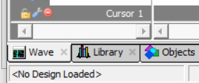
观察整个界面发现,左下角出现 No Design Loaded ,这是唯一给到的信息。于是去搜索各种解决办法,尝试之后均没有改变。
在这里插入图片描述

二、解决办法

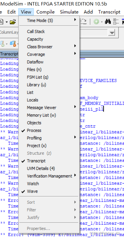
我们要想办法,让仿真软件能给我们提供更多信息,从而去纠错。如下图所示,点击View——transcript,就会出现各种运行记录,其中也会提示Error,就可以根据提示进行修改了。
在这里插入图片描述

我当时一直找不到错误的原因,仅仅是不出任何波形,对修改更是无处下手,看提示发现,仅仅是因为module中 多打了一个逗号!!!!不过也算学会了如何让仿真软件去显示更多的仿真信息。

三、modelsim不能自动出现波形

同样的,当quartus中调用modeslim仿真的时候,可能出现无波形的情况,这时候可以采用手动添加等方式,但如果手动添加仍然没有解决该问题,那么我们也要在transcript窗口中找错误,错误修改后,重新仿真即可。
有效参考

  • 9
    点赞
  • 10
    收藏
    觉得还不错? 一键收藏
  • 打赏
    打赏
  • 0
    评论
Publisher: Prentice Hall PTR Pub Date: September 15, 2003 ISBN: 0-13-066946-6 Pages: 608 Section 2.7. The Spectrum of an Ideal Square Wave Section 2.8. From the Frequency Domain to the Time Domain Section 2.9. Effect of Bandwidth on Rise Time Section 2.10. Bandwidth and Rise Time Section 2.11. What Does "Significant" Mean? Section 2.12. Bandwidth of Real Signals Section 2.13. Bandwidth and Clock Frequency Section 2.14. Bandwidth of a Measurement Section 2.15. Bandwidth of a Model Section 2.16. Bandwidth of an Interconnect Section 2.17. Bottom Line Chapter 3. Impedance and Electrical Models Section 3.1. Describing Signal-Integrity Solutions in Terms of Impedance Section 3.2. What Is Impedance? Section 3.3. Real vs. Ideal Circuit Elements Section 3.4. Impedance of an Ideal Resistor in the Time Domain Section 3.5. Impedance of an Ideal Capacitor in the Time Domain Section 3.6. Impedance of an Ideal Inductor in the Time Domain Section 3.7. Impedance in the Frequency Domain Section 3.8. Equivalent Electrical Circuit Models Section 3.9. Circuit Theory and SPICE Section 3.10. Introduction to Modeling Section 3.11. The Bottom Line Chapter 4. The Physical Basis of Resistance Section 4.1. Translating Physical Design into Electrical Performance Section 4.2. The Only Good Approximation for the Resistance of Interconnects Section 4.3. Bulk Resistivity Section 4.4. Resistance per Length Section 4.5. Sheet Resistance Section 4.6. The Bottom Line Chapter 5. The Physical Basis of Capacitance Section 5.1. Current Flow in Capacitors Section 5.2. The Capacitance of a Sphere Section 5.3. Parallel Plate Approximation Section 5.4. Dielectric Constant Section 5.5. Power and Ground Planes and Decoupling Capacitance Section 5.6. Capacitance per Length Section 5.7. 2D Field Solvers Section 5.8. Effective Dielectric Constant Section 5.9. The Bottom Line Chapter 6. The Physical Basis of Inductance Section 6.1. What Is Inductance? Section 6.2. Inductance Principle #1: There Are Circular Magnetic-Field Line Loops Around All Currents Section 6.3. Inductance Principle #2: Inductance Is the Number of Webers of Field Line Loops Around a Conductor per Amp of Current Through It Section 6.4. Self-Inductance and Mutual Inductance Section 6.5. Inductance Principle #3: When the Number of Field Line Loops Around a Conductor Changes, There Will Be a Voltage Induced Across the Ends of the Conductor Section 6.6. Partial Inductance Section 6.7. Effective, Total, or Net Inductance and Ground Bounce Section 6.8. Loop Self- and Mutual Inductance Section 6.9. The Power-Distribution System (PDS) and Loop Inductance Section 6.10. Loop Inductance per Square of Planes Section 6.11. Loop Inductance of Planes and Via Contacts Section 6.12. Loop Inductance of Planes with a Field of Clearance Holes Section 6.13. Loop Mutual Inductance Section 6.14. Equivalent Inductance Section 6.15. Summary of Inductance Section 6.16. Current Distributions and Skin Depth Section 6.17. High-Permeability Materials Section 6.18. Eddy Currents Section 6.19. The Bottom Line Chapter 7. The Physical Basis of Transmission Lines Section 7.1. Forget the Word Ground Section 7.2. The Signal Section 7.3. Uniform Transmission Lines Section 7.4. The Speed of Electrons in Copper Section 7.5. The Speed of a Signal in a Transmission Line Section 7.6. Spatial Extent of the Leading Edge Section 7.7. "Be the Signal" Section 7.8. The Instantaneous Impedance of a Transmission Line Section 7.9. Characteristic Impedance and Controlled Impedance Section 7.10. Famous Characteristic Impedances Section 7.11. The Impedance of a Transmission Line Section 7.12. Driving a Transmission Line Section 7.13. Return Paths Section 7.14. When Return Paths Switch Reference Planes Section 7.15. A First-Order Model of a Transmission Line Section 7.16. Calculating Characteristic Impedance with Approximations Section 7.17. Calculating the Characteristic Impedance with a 2D Field Solver Section 7.18. An n-Section Lumped Circuit Model Section 7.19. Frequency Variation of the Characteristic Impedance Section 7.20. The Bottom Line Chapter 8. Transmission Lines and Reflections Section 8.1. Reflections at Impedance Changes Section 8.2. Why Are There Reflections? Section 8.3. Reflections from Resistive Loads Section 8.4. Source Impedance Section 8.5. Bounce Diagrams Section 8.6. Simulating Reflected Waveforms Section 8.7. Measuring Reflections with a TDR Section 8.8. Transmission Lines and Unintentional Discontinuities Section 8.9. When to Terminate Section 8.10. The Most Common Termination Strategy for Point-to-Point Topology Section 8.11. Reflections from Short Series Transmission Lines Section 8.12. Reflections from Short-Stub Transmission Lines Section 8.13. Reflections from Capacitive End Terminations Section 8.14. Reflections from Capacitive Loads in the Middle of a Trace Section 8.15. Capacitive Delay Adders Section 8.16. Effects of Corners and Vias Section 8.17. Loaded Lines Section 8.18. Reflections from Inductive Discontinuities Section 8.19. Compensation Section 8.20. The Bottom Line Chapter 9. Lossy Lines, Rise-Time Degradation, and Material Properties Section 9.1. Why Worry About Lossy Lines Section 9.2. Losses in Transmission Lines Section 9.3. Sources of Loss: Conductor Resistance and Skin Depth Section 9.4. Sources of Loss: The Dielectric Section 9.5. Dissipation Factor Section 9.6. The Real Meaning of Dissipation Factor Section 9.7. Modeling Lossy Transmission Lines Section 9.8. Characteristic Impedance of a Lossy Transmission Line Section 9.9. Signal Velocity in a Lossy Transmission Line Section 9.10. Attenuation and the dB Section 9.11. Attenuation in Lossy Lines Section 9.12. Measured Properties of a Lossy Line in the Frequency Domain Section 9.13. The Bandwidth of an Interconnect Section 9.14. Time-Domain Behavior of Lossy Lines Section 9.15. Improving the Eye Diagram of a Transmission Line Section 9.16. Pre-emphasis and Equalization Section 9.17. The Bottom Line Chapter 10. Cross Talk in Transmission Lines Section 10.1. Superposition Section 10.2. Origin of Coupling: Capacitance and Inductance Section 10.3. Cross Talk in Transmission Lines: NEXT and FEXT Section 10.4. Describing Cross Talk Section 10.5. The SPICE Capacitance Matrix Section 10.6. The Maxwell Capacitance Matrix and 2D Field Solvers Section 10.7. The Inductance Matrix Section 10.8. Cross Talk in Uniform Transmission Lines and Saturation Length Section 10.9. Capacitively Coupled Currents Section 10.10. Inductively Coupled Currents Section 10.11. Near-End Cross Talk Section 10.12. Far-End Cross Talk Section 10.13. Decreasing Far-End Cross Talk Section 10.14. Simulating Cross Talk Section 10.15. Guard Traces Section 10.16. Cross Talk and Dielectric Constant Section 10.17. Cross Talk and Timing Section 10.18. Switching Noise Section 10.19. Summary of Reducing Cross Talk Section 10.20. The Bottom Line Chapter 11. Differential Pairs and Differential Impedance Section 11.1. Differential Signaling Section 11.2. A Differential Pair Section 11.3. Differential Impedance with No Coupling Section 11.4. The Impact from Coupling Section 11.5. Calculating Differential Impedance Section 11.6. The Return-Current Distribution in a Differential Pair Section 11.7. Odd and Even Modes Section 11.8. Differential Impedance and Odd-Mode Impedance Section 11.9. Common Impedance and Even-Mode Impedance Section 11.10. Differential and Common Signals and Odd- and Even-Mode Voltage Components Section 11.11. Velocity of Each Mode and Far-End Cross Talk Section 11.12. Ideal Coupled Transmission-Line Model or an Ideal Differential Pair Section 11.13. Measuring Even- and Odd-Mode Impedance Section 11.14. Terminating Differential and Common Signals Section 11.15. Conversion of Differential to Common Signals Section 11.16. EMI and Common Signals Section 11.17. Cross Talk in Differential Pairs Section 11.18. Crossing a Gap in the Return Path Section 11.19. To Tightly Couple or Not to Tightly Couple Section 11.20. Calculating Odd and Even Modes from Capacitance- and Inductance-Matrix Elements Section 11.21. The Characteristic Impedance Matrix Section 11.22. The Bottom Line Appendix A. 100 General Design Guidelines to Minimize Signal-Integrity Problems Section A.1. Minimize Signal-Quality Problems on One Net Section A.2. Minimize Cross Talk Section A.3. Minimize Rail Collapse Section A.4. Minimize EMI Appendix B. 100 Collected Rules of Thumb to Help Estimate Signal-Integrity Effects Section B.1. Chapter 2 Section B.2. Chapter 3 Section B.3. Chapter 4 Section B.4. Chapter 5 Section B.5. Chapter 6 Section B.6. Chapter 7 Section B.7. Chapter 8 Section B.8. Chapter 9 Section B.9. Chapter 10 Section B.10. Chapter 11 Appendix C. Selected References About the Author

“相关推荐”对你有帮助么?

  • 非常没帮助
  • 没帮助
  • 一般
  • 有帮助
  • 非常有帮助
提交
评论
添加红包

请填写红包祝福语或标题

红包个数最小为10个

红包金额最低5元

当前余额3.43前往充值 >
需支付:10.00
成就一亿技术人!
领取后你会自动成为博主和红包主的粉丝 规则
hope_wisdom
发出的红包

打赏作者

Fighting_FPGA

你的鼓励将是我创作的最大动力

¥1 ¥2 ¥4 ¥6 ¥10 ¥20
扫码支付:¥1
获取中
扫码支付

您的余额不足,请更换扫码支付或充值

打赏作者

实付
使用余额支付
点击重新获取
扫码支付
钱包余额 0

抵扣说明:

1.余额是钱包充值的虚拟货币,按照1:1的比例进行支付金额的抵扣。
2.余额无法直接购买下载,可以购买VIP、付费专栏及课程。

余额充值