


原文链接:https://www.quora.com/What-is-the-difference-between-HBM-High-Bandwidth-Memory-and-DDR-memory
Michael Sporer
My entire career is in semiconductor memories Answered Feb 24, 2017
DDR SDRAM memory are packaged components intended to be soldered to a board. These chips have either 4b, 8b or 16b datapath and a group of them are connected on a DIMM module to form a 64 bit datapath. These component packages usually contain only one chip inside, but can have more if you need higher capacity.
HBM is still DRAM on the inside of the chip, meaning the bitcell is the same, but almost everything else is different. Different chip architecture, different IO, different package technology.

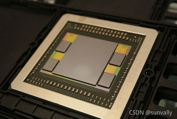
HBM is defined as a stack of HBM die where the die are connected using Through Silicon Via (TSV) interconnect. The interconnection of the die is used to build wide bus architectures. One HBM package can have up to 8 die stacked. The interface on the package consists of EIGHT 128b busses (called channels), each one uniquely controlled.
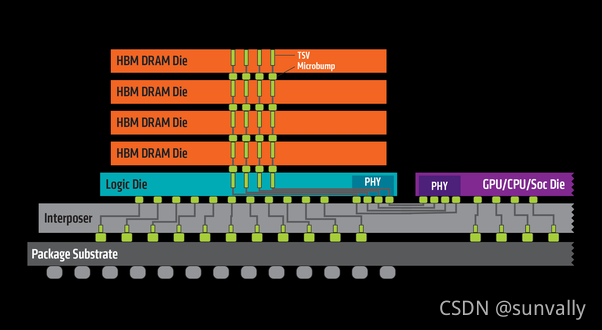
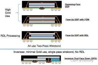
The pin count on HBM is very high and requires either direct attach or silicon interposer technology.
AMD is the industry pioneer to use 1st generation HBM on their GPU. Xilinx has extensive experience connecting chips together with Silicon interposer and has announce products that will use 2nd generation HBM. Nvidia and Intel/Altera have made some announcements about these kinds of technologies.
Indranil Sen
former Component Design Engineer at Intel (2014-2019) Answered Jun 3, 2018
Although a comprehensive answer has been given by Michael, I would just add to the differences between the two:
-
Packaging:
DDR memories are generally off-chip DIMMs (Dual In-line Memory Modules), which means they are separate from the CPU die and are at a distance away from the CPU on the motherboard (though the controller is usually packaged with the CPU die). HBM on the other hand, are packaged on top the CPU die using the Through Silicon Via (TSV) interconnects and can be stacked on top of each other. Thus, they are much closer to the CPU (or GPU) as compared to the DDR based DIMMs. -
Bandwidth:
This is actually where the advantage of HBM comes into the picture. HBM based DRAM memories, being part of the same package (on-die) as the processor can afford to have a large pin count (for Command, Address and Data) as compared to an off-die DIMM. If the pin count of a DIMM were to be increased (say for more parallel data access), the CPU package would also have to increase its pin count, making it unfeasible for signal transmission across the motherboard PCB. HBM being connected on die with TSVs, can afford a larger pin count, enabling a larger scale of parallel access of Data (wider bus with more channels), thereby boosting the bandwidth. -
Latency:
Again, HBM being closer to the processor die, offers lower latency compared to the DDR based DIMMs.
A point to note from 2 and 3 is, HBM provides a higher throughput (combination of bandwidth and latency), compared to a DDR based module.
- Capacity:
This is where DDR memory is the clear winner. Being a separate module altogether, it can pack in way more capacity even with 8 HBM based DRAM dies stacked on top of the CPU die.
- Protocol/PHY/IO design:
HBM is mostly a derived version of DDR in terms of the protocol (still uses dual edge data strobing), main difference being a wider data bus requiring more number of the DQS strobe generation, in addition to having more number of channels. The logic and electrical PHY and the IO design for HBM is different, owing to factors like the memory being close to the die, signal integrity and power issues while transmitting data across TSVs and also the shape of the DRAM die affects the floorplan of these designs (where the interconnects land on the die). This topic requires a separate discussion in itself.
From an application point of view, DDR based DRAM DIMMs are still used as the main system memory for most client and server systems, while HBM is used for applications that require low latency, high bandwidth but at the cost of a lower capacity. AMD has been actively using HBM for their discrete GPUs while some other semiconductor companies use the HBM based DRAMs as a separate local cache for high end applications in servers (AI, machine learning etc), for storing a large amount of data locally (than system memory), thereby giving performance boosts. Samsung has tried to use the Wide IO (similar to HBM) as system memory for Mobile SoCs.


 5294
5294

 被折叠的 条评论
为什么被折叠?
被折叠的 条评论
为什么被折叠?
 到【灌水乐园】发言


