


 本文详细介绍了Verilog中各种类型的延迟(如简单、聚集和条件延迟),以及如何在门级、数据流和行为级模型中指定这些延迟。此外,还讨论了$setup,$hold和$width等同步时序检查的用法。
Verilog provides language constructs to model any kind of delays. It can define simple delays, lumped delays and even conditional delays which are useful for circuits with multiplexed output. This post describes all delay types and how to specify them using verilog constructs.

Delays
Verilog provides language constructs to model any kind of delays. It can define simple delays, lumped delays and even conditional delays which are useful for circuits with multiplexed output.
A delay (in Verilog) is the amount of time (units) it takes to receive a response of the circuit. In combinational circuit this is the time units taken to obtain a value at output in response to the change in inputs. In sequential circuits, the delay is the time taken by the circuit to change the output from the triggering edge of the clock, rather than from the change in data values.
Delays for gate level modeling
There are three type of delays that can be specified for gates.
- Rise Delay: the time it takes to set an output high (0, z, x to 1)
- Fall Delay: the time it takes to set an output low (1, z, x to 0)
- Turn off delay: the time it takes to cut off a buffer (0, 1, x to z)
0, 1, z and x have their usual meanings as logic low, logic high, high impedance (floating gate) and unknown value. The fourth transition is to unknown value, i.e. 0, 1, z to x, and this is taken to be the minimum of other three. The turn off delay is specified only for tri-state devices. Although it is available for other gates, it is never used.
These delays are specified as:
gate_type #(t_rise, t_fall, t_off) gate_name (output, par1, ...)
Using the ‘#’ token, any or all of these delays can be specified:
- If only one value is specified, it is used for all three.
not # 2 n0(out, in); /* Rise=2, Fall=2, Turn-Off=2 */
- If two values are specified, they are used for rise and fall delay respectively. The turn off delay is taken to be minimum of these value.
and #(2,3) a0(out, a, b);  /* Rise=2, Fall=3, Turn-Off=2 */
and #(3,1) a0(out, a, b);  /* Rise=3, Fall=1, Turn-Off=1 */
- If all three values are specified they are taken respectively for rise, fall and turn off delays
Delay for dataflow modeling
In dataflow modeling the delays are associated with nets.
NET DECLARATION DELAY
The delay is associated with the net during its declaration. Any change to the signal will propagate only after the assigned delay.
wire #10 out;
assign out = a & b;
The input pulses shorter to the specified delay are filtered out. If the value of inputs change before the assignment has taken place, the assignment will not be carried. This is called as inertial delay.
REGULAR ASSIGNMENT DELAY
This is the delay associated with continuous assignment.
wire out;
assign #10 out = a & b;
IMPLICIT CONTINUOUS ASSIGMENT
This delay is associated with a net when it is implicitly assigned a value during its declaration.
wire #10 out = a & b;
Delays for behavioral modeling
See the paper for detailed description. The summary of coding guidelines is:
MODELING COMBINATIONAL LOGIC WITH PROCEDURAL ASSIGNMENTS
- When a combinational logic is modeled using blocking assignment, placing delay on the LHS of blocking assignment produces flawed hardware model. Similarly placing delays on RHS also results in wrong model. For example
module adder(input a, b, c_in, output sum, c_out);
  always @ (a or b or c_in)
    #15 {c_out, sum} = a + b + c_in;
endmodule

module adder(input a, b, c_in, output sum, c_out);
  always @ (a or b or c_in)
    {c_out, sum} = #12 a + b + c_in;
endmodule
will both produce a flawed model.
- Placing delay on LHS of nonblocking procedural assignment will model the wrong behavior. This is also a bad coding style.
module adder(input a, b, c_in, output sum, c_out);
  always @ (a or b or c_in)
    #15 {c_out, sum} <=  a + b + c_in;
endmodule
This model is flawed.
- Modeling combinational logic with nonblocking procedural assignment with delays added on RHS will accurately model the combinational logic with transport delays.
module adder(input a, b, c_in, output sum, c_out);
  always @ (a or b or c_in)
    {c_out, sum} <= #12 a + b + c_in;
endmodule
This coding style should be used to model behavioral delay-line logic.
However, this style also should not be used when multiple sequential nonblocking assignments are used to model combinational logic, unless all of the RHS input identifiers are listed in the sensitivity list, including the temporary variables in the always block.
module adder(input a, b, c_in, output sum, c_out);
  always @ (a or b or c_in or temp)
    temp <= #12 a + b + c_in;
    {c_out, sum} <= temp;
endmodule

module adder(input a, b, c_in, output sum, c_out);
  always @ (a or b or c_in)
    temp <= a + b + c_in;
    {c_out, sum} <= #12 temp;
endmodule
These styles can be confusing hence they should be avoided.
MODELING COMBINATIONAL LOGIC WITH CONTINUOUS ASSIGNMENT
Adding delay to continuous assignment accurately models the combinational logic with inertial delays and is recommended coding style. Since the continuous assignments do not add the output assignment to queues therefore they model combinational logic with inertial delays. They keep track of the next output value and when it will occur.
module adder (input a, b, c_in, output sum, c_out);
  assign #12 {c_out, sum} = a + b + c_in;
endmodule
A combinational model where the output of one continuous assignment drives the input of another continuous assignment also accurately models the logic.
Delay Modeling
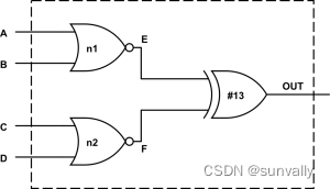
There are a number of ways to attribute delays to a circuit. The most commonly used techniques are distributed delay, lumped delay, and pin-to-pin delay.
Distributed delay
In this model the delays are assigned to every element of the circuit. The delay between any two points is calculated by adding the delays of the components through which the signal passes.
Distributed Delay Model
In the example circuit the first NOR gate has a delay of 4 units, the second has delay of 6 units and the XOR gate has delay of 7 units. When the input of any gate changes, the output changes after the specified delay.
The module can be declared as:
module circuit(input A, B, C, D, output OUT);
 wire E, F;
 nor #4 n1 (E, A, B);
 nor #6 n2 (F, C, D);
 xor #7 x1 (OUT, E, F);
endmodule
or as
module circuit(input A, B, C, D, output OUT);
 wire E, F;
 assign #4 E = A ~| B;
 assign #6 F = C ~| D;
 assign #7 OUT = E ^ F;
endmodule
The above modules have delays of 4+7 = 11 and 6+7 = 13 for the four connections from the input to output of circuit.
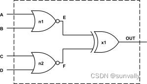
Lumped delay
In this model the delays are assigned to modules rather than their components. Normally the delay assigned to a module is the longest path delay to reflect the worst case. It is assigned mostly to the output port of the module. The above module with lumped delay is as follows:
Lumped Delay Circuit
As can be seen this reflects the worst case delay of 13. It can be written as:
module circuit(input A, B, C, D, output OUT);
 wire E, F;
 nor n1 (E, A, B);
 nor n2 (F, C, D);
 xor #13 x1 (OUT, E, F); /* Lumped delay at output gate */
endmodule
Pin to Pin delay (path delay method)
Path delays are specified from source (input or inout) pin to destination (output or inout) pin, rather than associating them with components. This does not requires the knowledge of details of internal components. They can be expressed in two ways:
- Conditional
- Non Conditional
Path delays are specified within a specify…endspecify block inside a module definition.
For our example circuit the code below shows how to associate path delays.
Pin to Pin delay Model
From the above example we know that the delays are as follows:
path A to E to OUT has delay 11 units
path B to E to OUT has delay 11 units
path C to F to OUT has delay 13 units
path D to F to OUT has delay 13 units
This can be specified as:
module circuit(input A, B, C, D, output OUT);
 wire E, F;
 nor n1 (E, A, B);
 nor n2 (F, C, D);
 xor x1 (OUT, E, F);

 specify
   ( A => OUT ) = 11;
   ( B => OUT ) = 11;
   ( C => OUT ) = 13;
   ( D => OUT ) = 13;
 endspecify
endmodule
NON CONDITIONAL PATH DELAYS
The above example code is a simple demonstration of how to associate pin to pin assignment delays. The pin to pin delays can be assigned in following ways:
- Parallel Connections: in this case each source and destination pin pair is assigned a delay. The source and destination ports should be same bit width, either single or multi bit vectors.
specify
  (in1 => out) = 6;
  (in2 => out) = 3;
endspecify
in1, in2, and out can be of single bit width as reg in1, in2, out; or of multibit width as reg [3:0] in1, in2, out;
- Full Connection: The *> notation may be used when every bit of the source port is to be associated with every bit of the destination port. The ports can be of different size.
reg [3:0] in;
reg [7:0] out;
specify
   ( in *> out ) = 9;
endspecify
- Using specparam: specparam is like local parameter to specify block. This is just for convenience. An example could be like:
specify
  specparam delay = 9;
  ( in *> out ) = delay;
endspecify
For a module with many paths, a mix of Parallel and Full connections can be used to assign the various delays.
The pin to pin timings can also be specified differently for different transitions. The order and and combination in which these can be specified is fixed. In any statement either 1, 2, 3, 6, or 12 values only can be specified. The combinations can be:
- If 1 parameter is specified it is used for all transitions
- If 2 parameters are specified, the first one is associated with rise time (0 to 1, 0 to z, z to 1) and second one with fall time (1 to 0, 1 to z, z to 0)
I- f 3 parameters are specified they are associated with rise time (0 to 1, 0 to z), fall time (1 to 0, 1 to z) and turn-off time (z to 0, z to 1) respectively - If 6 parameters are specified, they are associated in the following order: 0 to 1, 1 to 0, 0 to z, z to 1, 1 to z, and z to 0.
- If 12 parameters are specified, they are associated in the following order: 0 to 1, 1 to 0, 0 to z, z to 1, 1 to z, z to 0, 0 to x, x to 1, 1 to x, x to 0, x to z, and z to x
CONDITIONAL PATH DELAYS OR STATE DEPENDENT PATH DELAYS (SDPD)
Verilog allows the delays to be set up according to the state of control signals or input variables. If statement is used to specify conditional delays as:
if (<conditional_expression>) <path> = <delay_value>;
The conditional expression operands can be scalar or vector inputs, inout ports, registers and nets or part-selects. The operators used can be any bitwise, reduction, concatenation or conditional operator. The path description can contain both Parallel and Full connections. Verilog does not support the use of the else construct for use with the if statement for assigning Path Delays.
For example the delays can specified as:
specify
if (c) (c => out) = 12;
if (~c) (c => out) = 8;

if (a | b) (a => out) = 10;
if (~(a | b)) (a => out) = 12;

if ({a,b} == 2'b11) (b => out) = 16;
if ({a,b} != 2'b11) (b => out) = 13;
endspecify
Note that two conditional statements are assigned for each path to avoid the possibility of condition not being defined (to cover the else cases). This is done most efficiently by using an if statement to assign a delay to all the other cases not previously defined explicitly for each set of paths.
Sequential Timing Checks : $setup $hold and $width
Sequential elements such as flip flops have timing constraints in the form of setup and hold time. The setup time specifies the maximum time before the triggering clock edge of the flip flop before which the data must be stable at the input of the flip flop. The hold time specified the minimum time after the triggering clock edge of flip flop that the data must be stable at the input of flip flip. These timing constraints make sure that the data is properly sensed by the flip flop.
To facilitate the checking of these violations, verilog has a number of constructs, the most important ones are $setup, $hold and $width.
Syntax:
$setup(data_signal, clock_signal, time_limit)
the data_signal is checked against the clock_signal (which is used as reference). The time_limit specifies the minimum time required between the two events. The time period is before the clock edge. A violation occurs if t_clockevent – t_dataevent < time_limit. The data_signal and clock_signal must be declared as wires.
$hold(clock_signal, data_signal, time_limit)
again the data signal is checked against the clock signal. A violation occurs if t_dataevent – t_clockevent < time_limit. The time period is after the clock edge.
$width(reference_event, time_limit)
It checks the time elapsed between the reference_event and the next event on the same signal, if their width is less than time_limit, a violation occurs.
AN EXAMPLE SHOWING THE TIMING CHECKS FOR A D FLIP FLOP
In this example we have a D type Flip Flop clocked at 100Mhz (10ns). The data input has setup time of 2ns and hold time of 2 ns.
module dff(input clk, input d, output reg q);
  always @(posedge clk)
    q <= d;
endmodule

module dff_tb();
  reg clk, d; /* Inputs to Flip Flop */
  wire q;     /* Output from Flip Flop */

  /* Declaring wire type signals to be used in timing checks */
  wire clk_signal, d_signal;

  assign clk_signal = clk;
  assign d_signal = d;

  dff I (.clk(clk), .d(d), .q(q));

  initial clk = 0;
  always #5 clk = ~clk;

  specify
    $setup(d_signal, posedge clk_signal, 2);
    $hold(posedge clk_signal, d_signal, 2);
    $width(negedge d_signal, 3);
  endspecify

  initial begin
    d = 1'b1;
    #10 d = 1'b0;
    #6 d = 1'b1; /* Hold Violation */
    #8 d = 1'b0; /* Setup Violation */
    #9 d = 1'b1;
    #4 d = 1'b0;
    #1 d = 1'b1; /* width violation */
    #20 $stop;
  end
endmodule
Compiling and running with synopsys vcs it gives the following output:
"setuphold.v", 23: Timing violation in dff_tb
    $hold( posedge clk_signal:15, d_signal:16, limit: 2 );

"setuphold.v", 22: Timing violation in dff_tb
    $setup( d_signal:24, posedge clk_signal:25, limit: 2 );

"setuphold.v", 24: Timing violation in dff_tb
    $width( negedge d_signal:37,  : 38, limit: 3 );
The output shows 3 timing violations.
- First one is a hold violation. The check was specified at line 23 in source code. It tells that the positive edge of clock occurred at time 15th time unit and the input data signal changed its value at 16th time unit. The hold time limit was specified as 2 time units. This is clearly a timing violation since the data signal changed 1 time unit after the positive edge of the clock.
- The second one is a setup violation. The check was specified at line 22. The data signal changed value at 24th time unit and the positive edge of clock occurred at 25th time unit, so there is only a difference of 1 time unit whereas the setup time limit was specified as 2 time units.
- Third violation is the width violation. The timing check required the data signal to remain stable for 3 time units after the negedge i.e. whenever the data signal transitions from 1 to 0, it should not change its value for next 3 time units. The violation specifies that the negative edge occurred at 37th time unit and the signal changed again at 38th time unit.


 679
679

 被折叠的 条评论
为什么被折叠?
被折叠的 条评论
为什么被折叠?
 到【灌水乐园】发言


