


1.1 目录
(1)目录
(2)题目要求
(3)代码
(4)代码错误分析
1.2 题目要求
For each bit in a 32-bit vector, capture when the input signal changes from 1 in one clock cycle to 0 the next. "Capture" means that the output will remain 1 until the register is reset (synchronous reset).Each output bit behaves like a SR flip-flop: The output bit should be set (to 1) the cycle after a 1 to 0 transition occurs. The output bit should be reset (to 0) at the positive clock edge when reset is high. If both of the above events occur at the same time, reset has precedence. In the last 4 cycles of the example waveform below, the 'reset' event occurs one cycle earlier than the 'set' event, so there is no conflict here.
解释:通俗的意思就是输入一个in[31:0],每当输入的in中的某一位发生下降沿(就是位数据从1变为0)时就把out[31:0]的对应位置1。而且当reset为高电平时,要让out清零,但是只清零一个周期,然后就让out继续输出上一次的in[31:0].
对下图进行分析:当in[31:0]等于2(后四位为0010),然后下个周期变成e(后四位为1110)。此时0010变到1110,每一位都没有出现下降沿,所以out=0;然而当in[31:0]从e(后四位为1110)变成0(后四位为0000)时就有1、2、3位出现下降沿了,所以out的1、2、3位置1,输出out为e。当reset为高电平时对out置零一个周期,然后一个周期后out输出上一次in[31:0]的值即是2.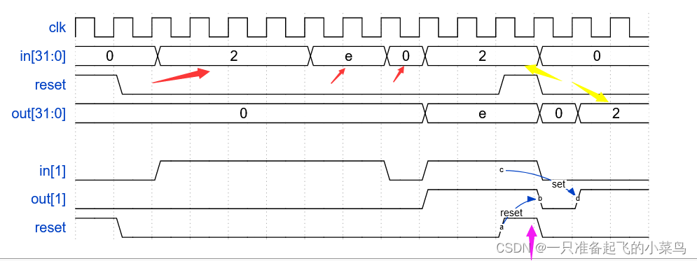
1.3 代码
//正确代码
module top_module (
    input clk,
    input reset,
    input [31:0] in,
    output [31:0] out
);
    reg [31:0]k;
    initial k=0;
    always@(posedge clk)
        k<=in;
    always@(posedge clk)
       if(reset)
           out<=0;
    	else
    		out<=~in&k|out;
endmodule
//错误代码
module top_module (
input clk,
input reset,
input [31:0] in,
output [31:0] out
);
reg [31:0]k;
initial k=0;
always@(posedge clk)
if(reset)
out<=0;
else
begin
k<=in;
out<=~in&k|out;
end
endmodule1.4 代码错误分析
运行错位代码出来的仿真图片如下: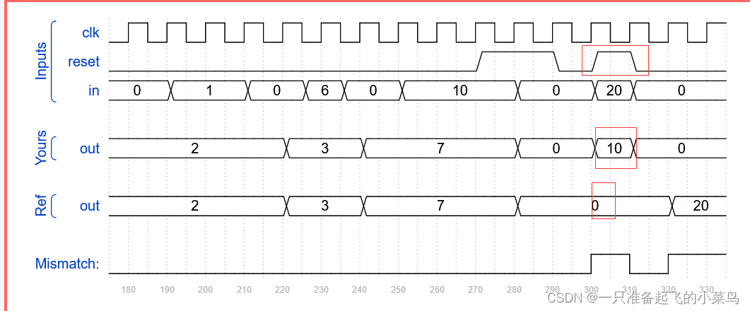
我们可以从图中发现我们的out输出在红框处和参考输出不一致,具体原因就是我们的我们out值在reset后输出的是,上一个reset时的值即是10,而题目要求因该是输出上一个in[31:0]的值,上一个in[31:0]值为0,所以我们应该输出0才对。
没有输出零的原因:就是我们的代码中对值进行存储不是每个周期都进行的,而题目要求应该是每个周期都进行存储的。我们当reset第一次高电平时,我们的错误代码没有执行k<=in;这行代码。所以导致我们没有把0给k而是把10给k,所以就导致在reset变低电平时out为10;
解决办法就是把k<=in;这行代码,单独用clk时钟运行。


 2247
2247


 被折叠的 条评论
为什么被折叠?
被折叠的 条评论
为什么被折叠?
 到【灌水乐园】发言


