


0 后仿的意义
对以下方面进行动态仿真确认
- 异步路径
- 时序紧张的同步路径
- 复位流程是否有时序问题
- 不定态扩散问题
1 后仿的方法流程
1.1 综合团队/后端团队release综合网表给DV进行仿真,这一步可以称为zero delay GLS(gate level simulation), 也可以干脆称为综合网表仿真。注意,不带延时反标的综合网表仿真,需要加上 nospecify 和 notimingcheck 这两个编译选项。
1.2 后端团队PR网表时序收敛得差不多的时候,用EDA工具提取出延时信息SDF,和PR网表一起release给DV,DV进行带延时反标的后端网表仿真,简称后仿。
SDF仿真不能加上的编译选项有:
nospecify: Supress module path delays and timing checks in specify blocks. So post simulation with SDF must remove this option.
notimingcheck: Supress timing checks in specify blocks.
no_notifier: Supress the togging of notifier registers that are optional auguments of systemveilog timing checks. The timing checks violation is no affected. 这个选项可以视具体情况而定,最好不要加上。
SDF仿真需要加上的编译选项有:
+neg_tchk: Enable negative timing checks. If you omit this option, VCS changes all negative limits to 0. Negative timing checks are either $setuphold timing check with negative setup or hold limits, or $recrem timing checks with negative recovery or removal tlimits.
-negdelay: Enable the use of negative values in IOPATH and INTERCONNECT entries in SDF files.
-sdfretain: Enable timing annotation as specified by a RETAIN retry on IOPATH delays.
1.3 SDF反标
SDF反标有两种方法
1) 使用VCS编译选项
-sdf min|typ|max:instance_name:file.sdf
2) 使用sdf_annotate()系统函数 -- 推荐
You can use the $sdf_annotate system task to back-annotate delay values from an SDF file to your Verilog design.
The syntax for the $sdf_annotate system task is as follows:
$sdf_annotate ("sdf_file"[, module_instance] [,"sdf_configfile"][,"sdf_logfile"][,"mtm_spec"] [,"scale_factors"][,"scale_type"]);
sdf_file: SDF文件
sdf_logfile: 指定SDF反标日志。默认情况下,VCS最多显示10条SDF反标警告到vcs compile log中。但是如果在这里指定了单独的反标日志,则所有的警告都会打到指定的日志中。
如果加了+sdfverbose编译选项,则vcs compile log中也会显示所有的反标警告。
"mtm_spec":
Specifies which delay values of min:typ:max triplets VCS MX back-annotates. Specify "MINIMUM", "TYPICAL", "MAXIMUM" or "TOOL_CONTROL" (default).
示例:
$sdf_annotate("xxx.sdf.gz", tb.dut, , annotate.log, "MAXIMUM");
以下是一些反标警告的分析总结:
Warning-[DRTZ] Detect delay value roundoff to 0
Delay from design or SDF file roundoff to 0 based in timescalue. Please check dumped diagnostic file (timescale.txt).
这个警告是由于cell的timescale没有设置好,可以查看timescale.txt, 分析cell的timescale是什么。
Warning-[SDFCOM_UHICD]
SDF Warning in instance
logic_mix.FE_OCPUNCOC97857_l2_connector_ram_1_1_data_mem_d_69_ of
module HD45_SH_BFX16:
/home/dspshop/amid/prime_power/tb14/glv_db/
logic_mix.fe_rut.try8.sdf.gz:192, SDF Warning: INTERCONNECT ->
accOutput(uphierarchy), port1 (Z) DEVICE delay applied
This warning is typically issued when one SDF interconnect delay has
to be backannotated on a net going from a device output to an output
port of one hierarchical block.
I believe Z is an output port and is connected to another output port
which is causing this warning message.
Please find the snippet from the sdf specifiacation3.0:
*****************************
3-21:
The INTERCONNECT entry is for the specification of interconnect delays
(actual or estimated) that are modeled independently for each driver-
to driven path. Both start and end points for the delay path are
specified.
Syntax
( INTERCONNECT port_instance port_instance delval_list )
The first port_instance is an output or bidirectional port.
The second port_instance is an input or bidirectional port.
delval_list is the INTERCONNECT delay between the output and input
ports.
当SDF的互联延时是从一个cell的output port到up hierarchy的某个输出port时就会报这个警告。因为SDF格式要求INTERCONNECT延时都是某个output/inout到某个input/inout的。
仿真器会将这种互联延时加到cell的device延时上面,从波形上看标上去的延时是符合预期的,所以这种警告可以忽略。
Warning-[SDFCOM_NICD]
SDF Warning: Negative INTERCONNECT Dealy
This negative value cannot be handled with switch -negdelay. Please check SDF files.
这种情况是由于SDF中的负interconnect延时不符合VCS的要求,即VCS在该负延时前后找不到正的延时进行合并处理。VCS user guide中说明如下:
To consider a negative INTERCONNECT delay, one of the following should be true:
-Sum of INTERCONNECT and PORT delays should be greater than zero
-Sum of INTERCONNECT and IOPATH delays should be greater than zero
-Sum of INTERCONNECT and DEVICE delays should be greater than zero
Otherwise, the negative INTERCONNECT delay is ignored, and a warning message is generated for the same.
Warning-[SDFCOM_ANICD] Adjust Negative INTERCONNECT DELAY
SDF Warning: Adjusting device delay for negative INTERCONNECT DELAY
tb.dut.U1234.X to
tb.dut.U1235.A
该警告的意思是说,将负的互联延时调整到前一个cell的IOPATH上了,提醒你注意一下!
比如,U1234.X->U1235.A的互联延时是-3ps, 而U1234的IOPATH A->X的delay原本是30,现在考虑到负的互联延时,就把U1234的IOPATH调整成30-3=27ps.
要知道EDA工具是很难模拟负延时的,因此只能将负的互联延时合并到前一级cell的IOPATH进行处理。因此就必须要求互联延时+前一级IOPATH延时>0.
Warning-[NTCDNC] Negative Timing Check Did Not Converge
Negative timing check delays did not converge, trying to solve by setting minimum constraint to zero.
当2个以上的timing check使用同一个reference event(比如 posedge ck),且这些timing check检查的时间窗口没有重合时,EDA工具没办法处理这种情况,即负延时检查没有收敛。
EDA工具会尝试把最小的一个负值改成0,去尝试解决这个问题。这样做会比原始的检查更为严格,所以是对仿真无害的。
1.4 DUT内部变量的初始化
网表内部难免有些寄存器是没有复位端或者置位端的,而这些寄存器的Q端在系统复位完后还是处于X态,一旦时钟跑起来,这些X态就有可能传播出去了。
因此,在项目实践中,可以让后端提供一个 no reset reg list, 他们可以用脚本非常方便的提取出来。有了这样一个list后,我们在后仿中可以对这些没有复位端的寄存器进行初始化。
1) 用vcs config file进行初始化
+vcs+initreg+config+config_file
Specifies a configuration file for initializing Verilog variables, registers defined in sequential UDPs, and memories including multi-dimensional arrays (MDAs) in your design, at time zero. In the configuration file, you can define the parts of a design to apply the initialization and the initialization values of the variables.
The syntax of the configuration file entries are:
defaultvalue x|z|0|1|random|random seed_value
instance instance_hierarchical_name [x|z|0|1|random| random seed_value]
tree instance_hierarchical_name depth [x|z|0|1|random| random seed_value]
module module_name [x|z|0|1|random|random seed_value]
modtree module_name depth [x|z|0|1|random|
random seed_value]
在config file中可以这样写
instance tb.dut.reg_0 random
tree tb.dut.xxx_inst 0 random
注意!这种方式只能初始化UDP(User Defined Primitives)中的reg。
You can use the +vcs+initreg+random option to initialize all bits of Verilog variables and registers defined in sequential UDPs and memories including multi-dimensional arrays (MDAs) in your design to random value 0 or 1, at time zero.
2) 用$deposit系统函数 - 推荐
$deposit(tb.dut.reg_0.Q, uramdom_range(0, 1) );
至于Memory, 可以将其所有单元的值初始化为随机值,也可以不初始化,具体视情况而定。比如,芯片的软件有时候会在网memory里写入值之前先读取memory的值,如果有这种情况,为了防止X态的传播,就必须先将Memory单元初始化为随机值。
1.5 X态问题的分析定位
没有遇到X态问题的后仿是不完整的。遇到X态不要慌,试着从以下几个角度分析。
1) 是否所有的DUT input端口都给予了一个known的值。
2) 是否对没有复位端的寄存器作了初始化。
3) DUT里有哪些Memory, 是否有必要进行初始化?
4) 如果是Timing violation引起的X态,则需要先分析Timing violation
5) 实在不行,就只能一级一级往前追了,找到X态源头
1.6 Timing violaton analyze and waive
对于原本就是工作在异步路径下的sync cell, 静态时序分析时没有对它们进行约束和分析,因此在动态仿真时也一定会出现Timing Violation.
可以让后端给一个sync cell的list, DV将其整理成notiming config file.
在编译选项中 +optconfigfile=noTiming.cfg
在noTiming.cfg中
instance {tb.dut.u_xxx} {noTiming};
另外,对于模块级或者子系统级的后仿,需要让后端给一个input delay, 即输入的数据信号相对于时钟信号的延时,然后DV根据这个input delay去驱动数据信号。
这个input delay可能会影响模块第一级触发器的时序!
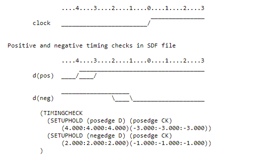
1.7 Negative timing check
负的setup/hold time到底是什么意思呢?
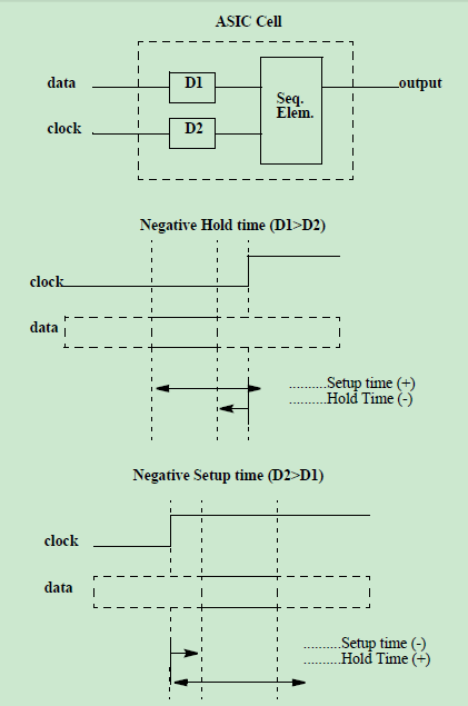
当ASIC Cell内部有时序器件,而Cell的输入时钟和输入数据到这个时序器件是有延时的,而且当我们以ASIC Cell为边boundary去进行timing检查时,
就有可能出现负的setup/hold time. 具体见上图。


 2774
2774

 被折叠的 条评论
为什么被折叠?
被折叠的 条评论
为什么被折叠?
 到【灌水乐园】发言


