


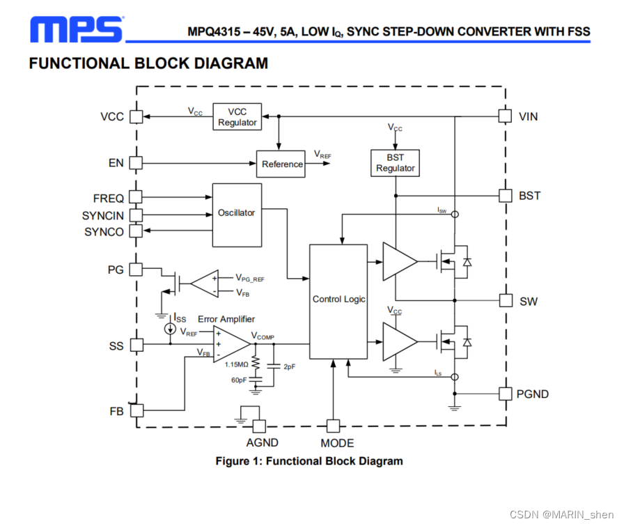
1,原理图和功能框图的设计:
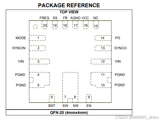
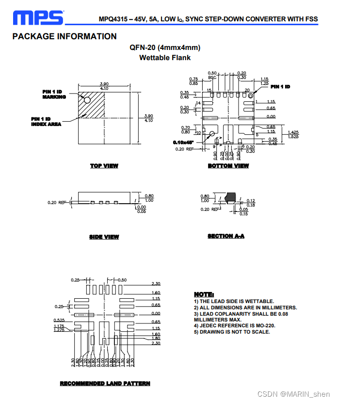
2,封装设计:
3,Layout设计需要注意点:我们从布局和布线上两个点来分析:
布局:
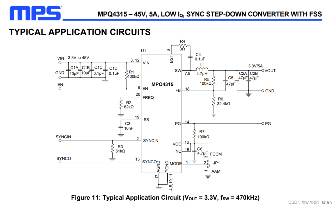
A, 输入滤波电容对称摆放在VIN和GND管脚附近。这个芯片手册上也是有提及的:
Place symmetric input capacitors as close as possible to the VIN and GND pins.

若是输入的电容有很多的话,板子布局的空间还不够,可以把预留的电容或者的大电容放置在背面(前提是大容值的放置在背面要满足板子的结构限高要求的),小容值的尽量保持和电源芯片在同一面。

.Place the ceramic input capacitor, especially the small package size (0603) input/output bypass capacitor, as close as possible to the PVIN/PVOUT and PGND pins to minimize high-frequency noise(放置陶瓷输入电容器,尤其是小包装尺寸(0603)输入/输出旁路电容器尽量靠近PVIN/PVOUT和PGND引脚,以最大限度地减少高频噪声)。
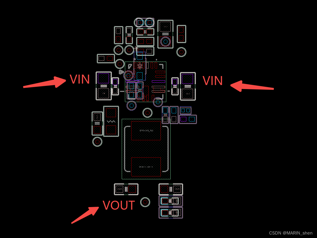
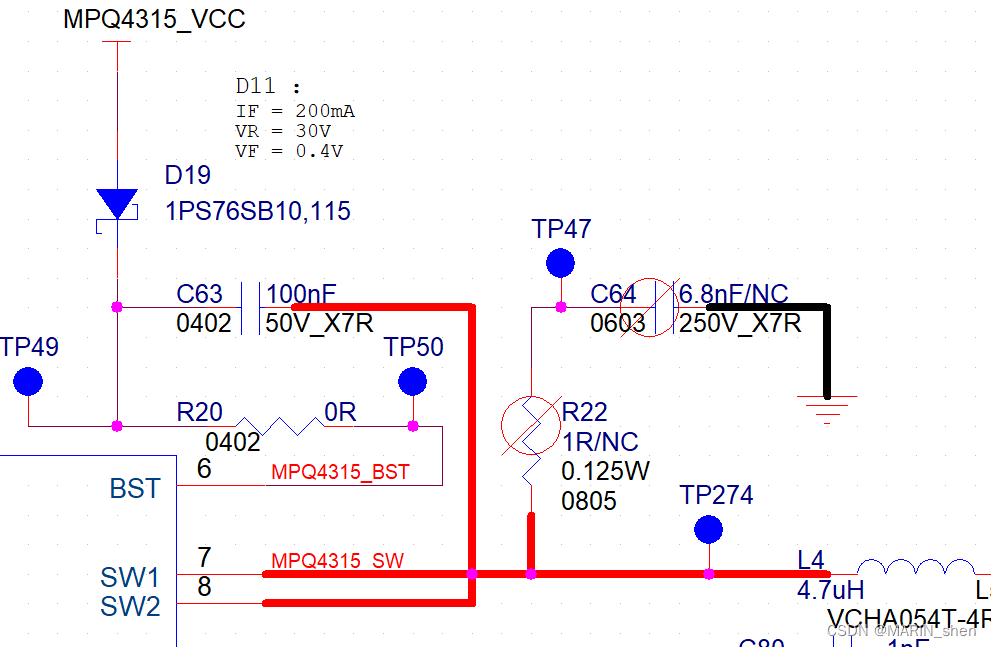
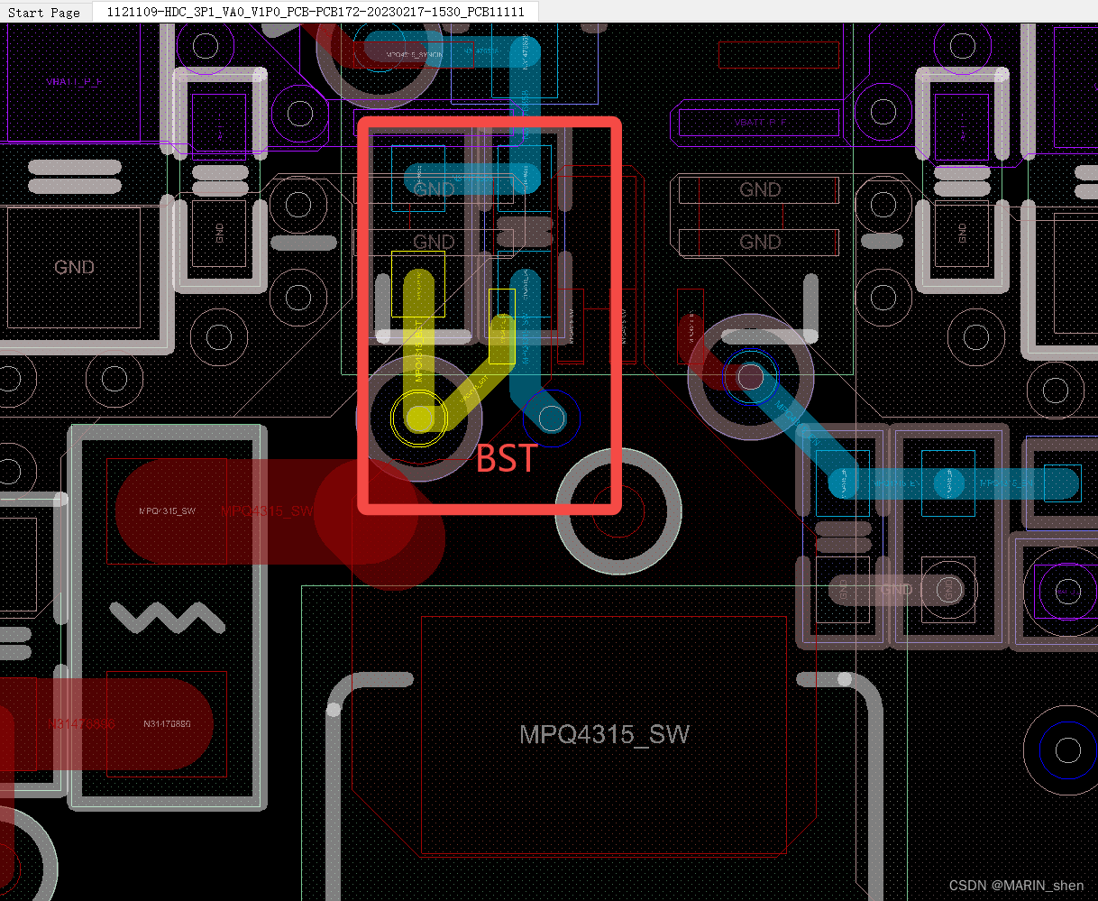
B, BST回路尽量短,器件尽量放置在和芯片同一面,有空间的前提下。
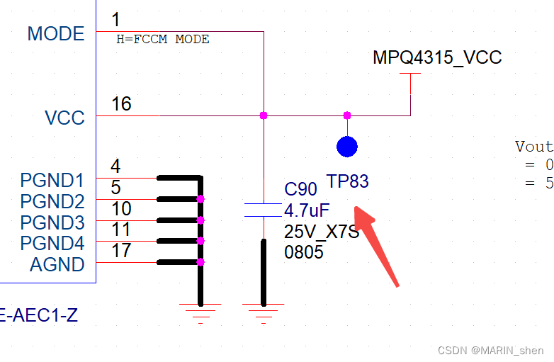
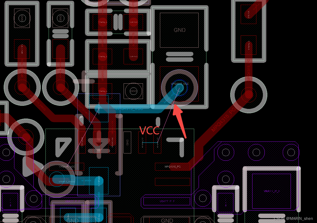
C,VCC电容尽量靠近相应的电源管脚放置,小容值的电容优化靠近电源管脚放置。
(Place the VCC capacitor as close to the VCC and GND pins as possible.)
D,FB的信号的阻容器件尽量靠近反馈管脚放置,尽量和芯片放置在同一面。(Place the feedback resistors close to the IC to keep the trace that connects to FB as short as possible.)

布线:
A,输入和输出的电源管脚铺铜皮尽量宽一些,电源孔可以多打一些(实际按照输入的电流大小来决定),内层也要补上电源铜皮(Keep the connection of the input capacitor
and VIN as short and wide as possible, Ensure that the high-current paths at GND
and VIN have short, direct, and wide traces, Use multiple vias to connect the power
planes to the internal layers.)
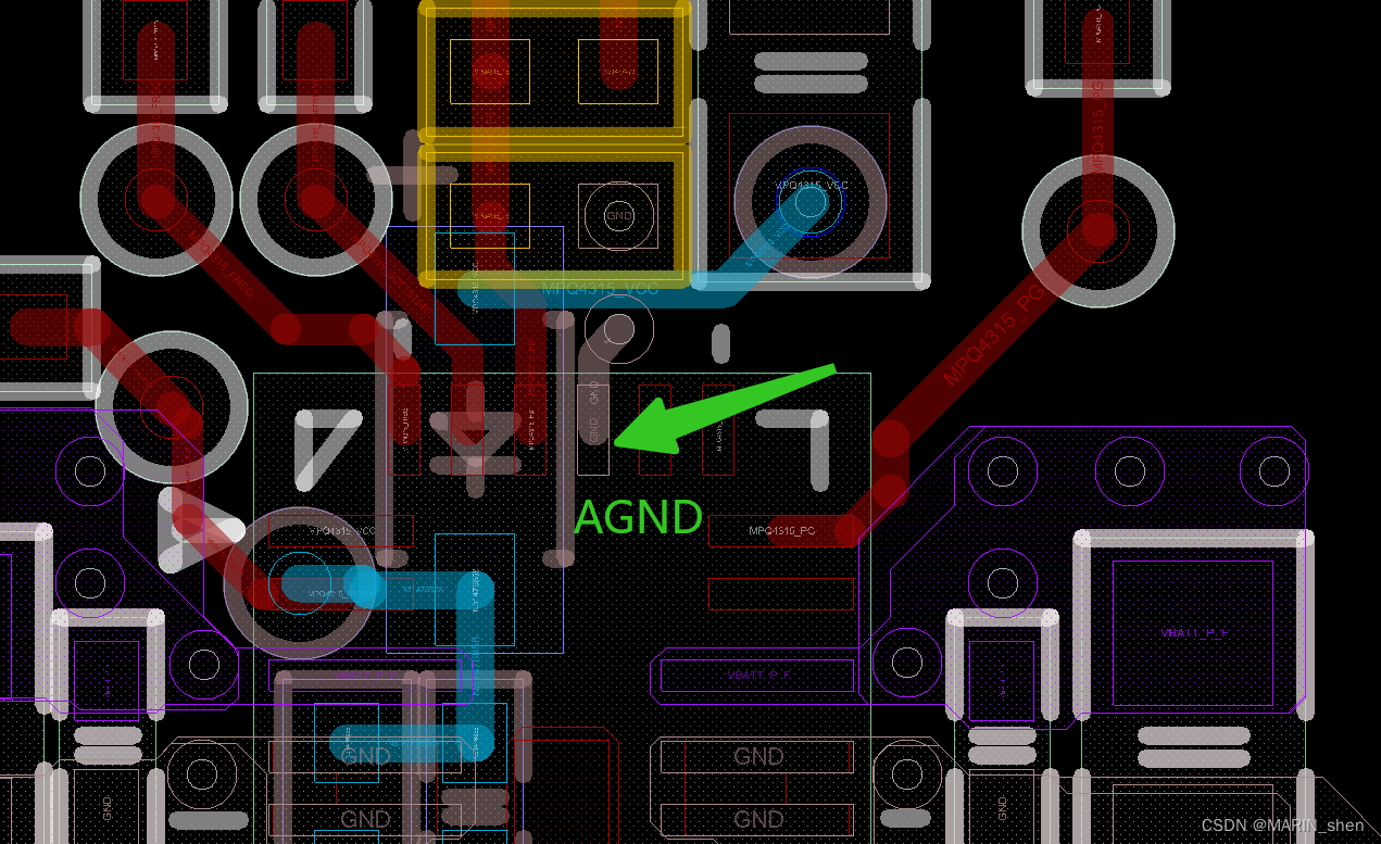
B,GND管脚的处理, 在GND管脚上用大的平面铺铜皮处理,可以多打一些GND via,但是前提是要保证内层的电源铜皮通道不被打VIA碎掉。(Use a large ground plane to connect directly to PGND. If the bottom layer is a ground plane, add vias near PGND.)

特别注意的GND还有AGND的处理,手册上也是有提到这个PIN脚的处理方法的,就是做单点GND处理,不要和PGND接上再去打孔。
![]()
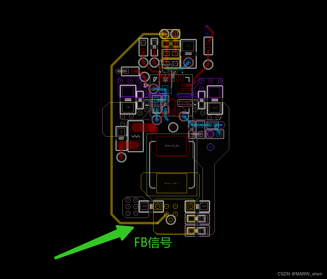
C,反馈FB管脚的处理,走线加粗,尽量远离其他敏感干扰信号,在输出电容末端采样比较好。
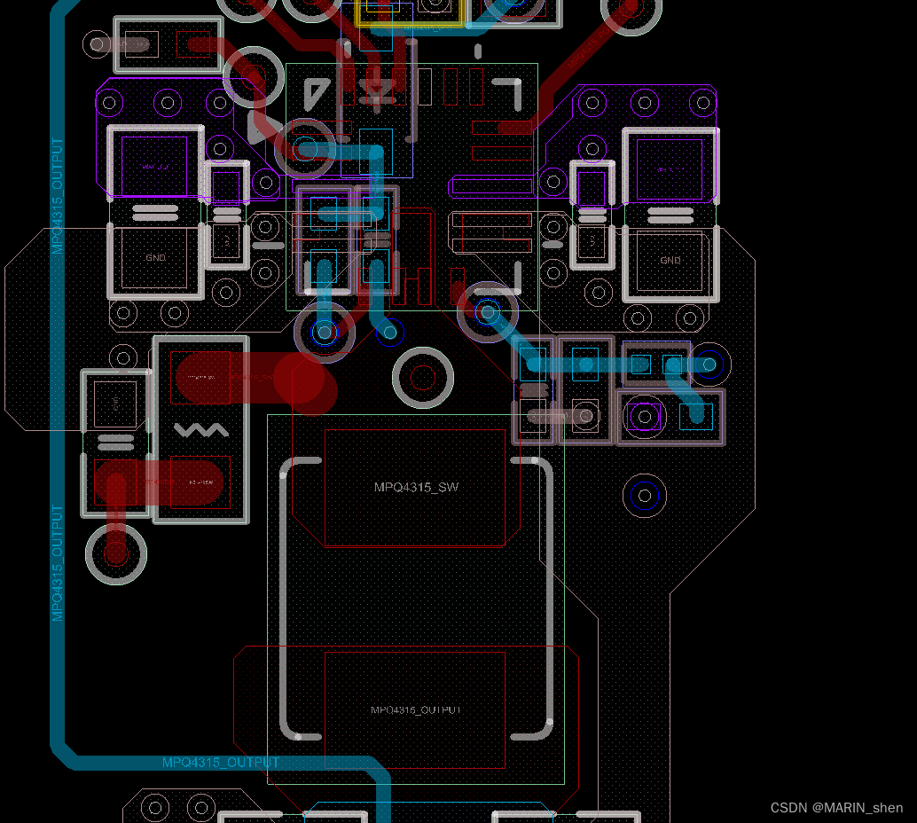
D,SW区域尽量不要穿其他敏感和高速信号。(Route SW and BST away from sensitive
analog areas, such as FB.)
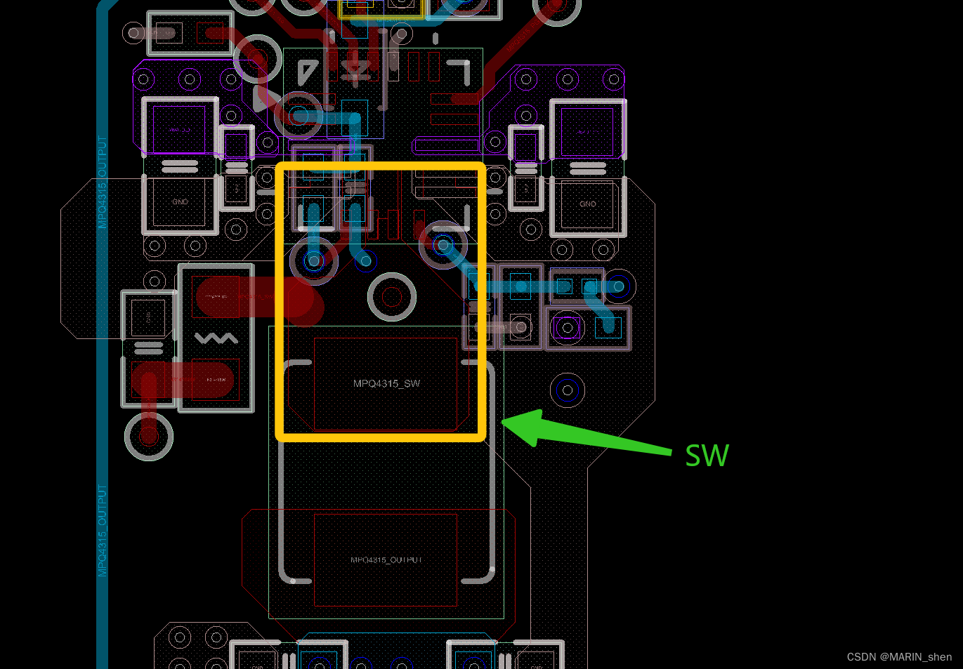
E,BST信号走线加粗处理,尽量远离其他敏感干扰信号。布线的时候要注意这个信号的布线回路尽量短。

以上就是小编在处理MPQ43155芯片的一些设计经验心得,若其中有不足之处,还望大师们指点一二。


 463
463


 被折叠的 条评论
为什么被折叠?
被折叠的 条评论
为什么被折叠?
 到【灌水乐园】发言


