analog IC layout-Design for reliability

集成电路是极为复杂的器件,几乎不可能达到完美,大多数器件都存在微小的不足和缺陷并导致失效,这一部分器件会在多年工作后突然无法继续使用,工程师们在可靠性实验中发现这些问题,在极端工作环境下可以加速老化来发现这些问题,但是并不是每一个设计缺陷都可以通过测试来发现,为了避免这些问题,版图绘制者要时刻牢记失效机制,并在版图绘制中考虑全面,从源头上减少失效的发生。

失效机制:

1、电迁移现象

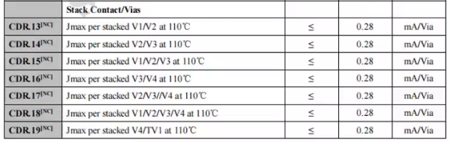
电迁移现象电迁移现象是因为极高电流密度产生的慢性损耗,主要原因是因为走线过窄导致。所以在版图设计过程中对于大电流的走线一定要根据金属过电流能力留出一定的金属宽度余量以防止出现电迁移失效。

根据LDO的带载能力,估计金属线宽度。
在这里插入图片描述

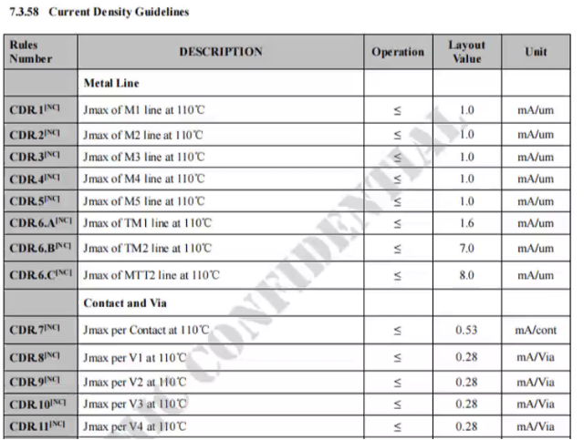
1、从工艺层面进行改进,为了改善电迁移现象,在大部分的金属互连中,使用的金属材料是铝,为了提高金属走线的过电流能力,一般会参杂一定比例的铜。
2、从版图层面进行改进,在版图绘制过程中就需要版图设计者对大电流的走线设置合理的走线线宽,保证芯片在极限工作环境下满足过电流要求。
在这里插入图片描述

2、天线效应

2、天线效应在干法刻蚀的时候会在晶片表面淀积电荷,如果连接到绝缘栅极的走线过长,在刻蚀的过程中,过长的走线就像是一条天线,收集刻蚀产生的静电荷。由于MOS器件属于压控型器件,栅极为绝缘氧化物,没有电荷泄放路径,不断积累的电荷达到一定程度后,就会对栅极造成介质击穿,这就是天线效应。

“天线”收集的电荷量主要由走线面积决定,由此可知天线效应主要与栅极面积和连接到栅极走线的面积相关,在设计规则文件中都会给出天线效应的计算公式,也可以直接通过运行天线效应设计规则文件进行检查。

预防天线效应
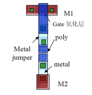
:1、金属走线跳线来消除天线效应,因为芯片的制造是一层一层不断通过淀积和刻蚀来完成的,通过“向上跳线法”将金属走线往更高的层走线可以消除天线效应。
在这里插入图片描述

2、如果金属走线跳线到顶层依然无法消除天线效应,这个时候就需要添加(N+/PSUB或P+/Nwell)二极管来消除天线效应的影响。

  • 0
    点赞
  • 5
    收藏
    觉得还不错? 一键收藏
  • 0
    评论
Authors: Dana Crowe & Alec Feinberg 1. Reliability Science 1.1 Introduction 1.2 Reliability Design: “A Stage Gate Approach” 1.3 Design for Reliability Tools 1.4 Reliability Verification 1.5 Analytical Physics 1.6 The Goal Is Customer Satisfaction 2. Understanding Customer Requirements 2.1 Introduction 2.2 Specified and Unspecified Requirements 2.3 Cost of Reliability 2.4 Benchmarking 2.5 Using Failure Modes and Effects Analysis to Meet Customer Requirements 3. Design Assessment Reliability Testing 3.1 Introduction 3.2 Four-Corner HALT Testing 3.3 Design Assessment Reliability Testing at the Hybrid and Component Level 3.4 Summary 4. Design Maturity Testing (DMT) 4.1 Introduction 4.2 Overview of DMT Planning 4.3 DMT Reliability Objectives 4.4 DMT Methods 4.5 Reliability and Sampling Distribution Models 4.6 Sample Size Planning 4.7 Automated Accelerated Test Planning 4.8 DMT Methodology and Guidelines References 5. Screening and Monotoring 5.1 Introduction 5.2 Achieving Reliability Growth in a Screening Program 5.3 Monitoring and Screening Tools 5.4 Highly Accelerated Stress Screening (HASS)Section II: Supporting Stage Gate Authors: Carl Bunis & Peter Ersland 6. Semiconductor Process Reliability 6.1 Introduction 6.2 Overview of Semiconductor Process Reliability Studies in the GaAs Industry 6.3 Wafer Level Reliability Tests 6.4 Summary References 7. Analytical Physics 7.1 Introduction 7.2 Physics of Failure 7.3 Analysis Flow 7.4 Failure Analysis Example 7.5 Analytical Techniques References Section III: Topics in Reliability Authors: Dana Crowe & Alec Feinberg 8. Reliability Statistics Simplified 8.1 Introduction 8.2 Definitions and Reliability Mathematics 8.3 Failure Rate Concepts 8.4 Reliability Models 8.5 Reliability Objectives and Confidence Testing 8.6 Parametric and Catastrophic Methods 8.7 Influence of Acceleration Factors on Test Planning References Appendix A – AT&T and Common Weibull Model Comparisons Appendix B – Helpful Microsoft® Excel Functions 9. Concepts in Accelerated Testing 9.1 Introduction 9.2 Common Sense Guidelines for Preventing Anomalous Accelerated Testing Failures 9.3 Time Acceleration Factor 9.4 Applications to Accelerated Testing 9.5 High-Temperature Operating Life Acceleration Model 9.6 Temperature-Humidity-Bias Acceleration Model 9.7 Temperature Cycle Acceleration Model 9.8 Vibration Acceleration Model 9.9 Electromigration Acceleration Model 9.10 Failure-Free Accelerated Test Planning 9.11 Step-Stress Testing 9.12 Describing Life Distributions as a Function of Stress 9.13 Summary References10. Accelerated Reliability Growth 10.1 Introduction 10.2 Estimating Benefits with Reliability Growth Fixes 10.3 Accelerated Reliability Growth Methodology 10.4 Applying Accelerated Reliability Growth Theory 10.5 Assessing Reliability Growth 10.6 Summary References Appendix – Accelerated Reliability Growth Stage Gate Model 11. Reliability Predictive Modeling 11.1 Introduction 11.2 System Reliability Modeling 11.3 Customer Expectations 11.4 Various Methods 11.5 Common Problems References Appendix A – Tabulated k of n System Effective Failure Rates Appendix B – Redundancy Equation with and without Repair Appendix C – Availability 12. Failure Modes and Effects Analysis 12.1 Failure Modes and Effects Analysis 12.2 FMEA Goal and Vision 12.3 FMEA Concepts 12.4 Types of FMEA Evaluations 12.5 Objectives 12.6 An FMEA Example 12.7 Implementation Methods Appendix A – Guide to Assigning FMEA Key Criteria Appendix B – FMEA Forms 13. Evaluating Product Risk 13.1 Introduction 13.2 Goals of a Risk Program 13.3 Managing Risks for Your Program 13.4 Four Steps to Risk Management 13.5 Guidelines for Risk Planning (Step 1) 13.6 Guidelines for Risk Assessment (Step 2) 13.7 Guidelines for Risk Analysis (Step 3) 13.8 Guidelines for Risk Handling (Step 4) 14. Thermodynamic Reliability Engineering 14.1 Thermodynamics and Reliability Engineering 14.2 The System and Its Environment 14.3 The Aging Process 14.4 Aging Due to Cyclic Force 14.5 Corrosion and Activation 14.6 Diffusion 14.7 Transistor Aging of Key Device Parameters 14.8 Understanding Logarithmic-in-Time Parametric Aging Associated with Activated Processes 14.9 Summary References
CMOS IC设计可靠性-回顾 CMOS集成电路(IC)是目前广泛应用于各种电子设备的一种主要技术。为了确保CMOS IC在长期使用和恶劣环境条件下的可靠性,设计工程师需要考虑多种因素。 首先,CMOS IC设计可靠性评估通常从设计阶段开始。在设计阶段,针对电路布局和布线等关键方面,需要考虑到电信噪声、电源噪声以及热效应等潜在的可靠性问题。通过合理的电路设计和布局,可以减少电路的噪声耦合和热点问题,提高可靠性。 其次,在CMOS IC设计,工艺参数和材料选择也会对可靠性产生影响。工程师需要了解不同工艺下的可靠性差异,并选择适合可靠性要求的工艺。例如,选择合适的氧化物薄膜和金属材料,可以有效减少漏电流和电子迁移等问题。 此外,可靠性测试和模拟也是评估CMOS IC设计可靠性的重要手段。通过在设计前进行可靠性仿真和电路测试,可以发现潜在的可靠性问题,并采取相应的优化措施。同时,设计工程师还需要对IC的寿命进行估计和预测,以便更好地了解其可靠性。 最后,CMOS IC可靠性还与电源管理和温度管理等因素密切相关。合理的电源管理和温度控制能够减少电流波动、温度变化和电压峰值等问题,从而提高CMOS IC可靠性。 综上所述,CMOS IC设计的可靠性评估是一个复杂而重要的过程。通过综合考虑设计阶段、工艺选择、可靠性测试和模拟以及电源管理等多个方面的因素,可以最大限度地提高CMOS IC可靠性。只有确保了CMOS IC可靠性,才能真正保证其在各种应用的稳定和可靠运行。

“相关推荐”对你有帮助么?

  • 非常没帮助
  • 没帮助
  • 一般
  • 有帮助
  • 非常有帮助
提交
评论
添加红包

请填写红包祝福语或标题

红包个数最小为10个

红包金额最低5元

当前余额3.43前往充值 >
需支付:10.00
成就一亿技术人!
领取后你会自动成为博主和红包主的粉丝 规则
hope_wisdom
发出的红包
实付
使用余额支付
点击重新获取
扫码支付
钱包余额 0

抵扣说明:

1.余额是钱包充值的虚拟货币,按照1:1的比例进行支付金额的抵扣。
2.余额无法直接购买下载,可以购买VIP、付费专栏及课程。

余额充值