


最近用Verilog HDL设计了一个小电路,一个3分频的电路,用的是我刚接触FPGA时,别人告诉我的思路,没想到今天才发现有大问题?
如下:
module Freq_divide(
	input clk,
	input rst_n,
	output reg clk_divide

    );

	wire clk_reverse;
	assign clk_reverse = ~clk;

	reg [3:0] count;
	always @ (posedge clk or posedge clk_reverse or negedge rst_n) begin
		if(!rst_n) begin
			count <= 0;
		end
		else if(count < 2) begin
			count <= count + 1;
		end
		else begin
			count <= 0;
		end
	end

	always @ (posedge clk or posedge clk_reverse or negedge rst_n) begin
		if(!rst_n) begin
			clk_divide <= 0;
		end
		else if(count == 2) begin
			clk_divide <= ~clk_divide;
		end
		else begin
			clk_divide <= clk_divide;
		end

	end


endmodule
这段代码确实是一个反面教材呀,为了偷懒,只是仿真了一下,觉得功能没有问题,还很满意,但是今天偶然的一次机会,我突然想看下RTL电路图,Vivado却报错了?
报错如下:
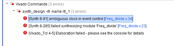
意思就是我的这句代码有问题:
always @ (posedge clk or posedge clk_reverse or negedge rst_n)
通过这种方式来实现双时钟采样是不对的。
这是问大神的聊天记录:

 最低0.47元/天 解锁文章


 3893
3893

 被折叠的 条评论
为什么被折叠?
被折叠的 条评论
为什么被折叠?
 到【灌水乐园】发言


