第二章数字电路时序分析---时序路径

数字电路时序分析

第一章 数字电路时序分析—建立保持时间
第二章 数字电路时序分析—时序路径


时序路径

时序路径是要进行时序分析的前提,想要进行时序分析,需要了解时序路径由那几部分组成

在这里插入图片描述

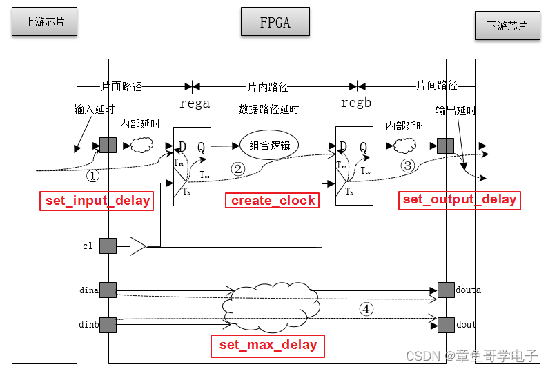
典型的时序路径有4类,如上图所示,这4类路径可分为片间路径(标记①和标记③)和片内路径(标记②和标记④)。

  1. 上游芯片到FPGA路径
  2. FPGA内部路径
  3. FPGA到下游芯片
  4. 上游芯片到下游芯片

我们一般只关注前三个。

1、上游芯片到FPGA路径

上游芯片到fpga的路径是输入端口到fpga第一集触发器的路径,在fpga中一般是使用set_input_delay进行约束。set_input_delay约束是约束时钟和数据的相位关系,相对延时多少,是边沿对齐还是中心对齐,是SDR单边沿信号还是DDR双边沿信号。

# Edge-Aligned Rising Edge Source Synchronous Inputs 
# (Using a direct FF connection)
#
# For an edge-aligned Source Synchronous interface, the clock
# transition occurs at the same time as the data transitions.
# In this template, the clock is aligned with the beginning of the
# data. The constraints below rely on the default timing
# analysis (setup = 1 cycle, hold = 0 cycle).
#
# input    __________                  ________________
# clock              |________________|                |__________
#                                     |
#                             skew_bre|skew_are 
#                             <------>|<------> 
#             ________________        |        ________________
# data     XXX________________XXXXXXXXXXXXXXXXX____Rise_Data___XXX
#

set input_clock         <clock_name>;      # Name of input clock
set input_clock_period  <period_value>;    # Period of input clock
set skew_bre            0.000;             # Data invalid before the rising clock edge
set skew_are            0.000;             # Data invalid after the rising clock edge
set input_ports         <input_ports>;     # List of input ports


# Input Delay Constraint
set_input_delay -clock $input_clock -max [expr $input_clock_period + $skew_are] [get_ports $input_ports];
set_input_delay -clock $input_clock -min [expr $input_clock_period - $skew_bre] [get_ports $input_ports];

# Report Timing Template
# report_timing -from [get_ports $input_ports] -max_paths 20 -nworst 1 -delay_type min_max -name src_sync_edge_rise_in  -file src_sync_edge_rise_in.txt;

这样以xilinx的SDR边沿对齐举例,set_input_delay的意思是数据相对时钟延时多少时间。

2、FPGA内部路径

FPGA内部路径是内部的逻辑之间的约束,一般只需要约束时钟,就是create_generated_clock,只需要高速综合工具,比如vivado需要跑多块的时钟就可以了。

3、FPGA到下游芯片路径

fpga到下游芯片路径是fpga的信号通过引脚将时钟和数据输出出去,这里以源同步系统为举例,使用set_output_delay进行约束。


#  Rising Edge Source Synchronous Outputs 
#
#  Source synchronous output interfaces can be constrained either by the max data skew
#  relative to the generated clock or by the destination device setup/hold requirements.
#
#  Setup/Hold Case:
#  Setup and hold requirements for the destination device and board trace delays are known.
#  
# forwarded         ____                      ___________________ 
# clock                 |____________________|                   |____________ 
#                                            |
#                                     tsu    |    thd
#                                <---------->|<--------->
#                                ____________|___________
# data @ destination    XXXXXXXXX________________________XXXXX
#
# Example of creating generated clock at clock output port
# create_generated_clock -name <gen_clock_name> -multiply_by 1 -source [get_pins <source_pin>] [get_ports <output_clock_port>]
# gen_clock_name is the name of forwarded clock here. It should be used below for defining "fwclk".	

set fwclk        <clock-name>;     # forwarded clock name (generated using create_generated_clock at output clock port)        
set tsu          0.000;            # destination device setup time requirement
set thd          0.000;            # destination device hold time requirement
set trce_dly_max 0.000;            # maximum board trace delay
set trce_dly_min 0.000;            # minimum board trace delay
set output_ports <output_ports>;   # list of output ports

# Output Delay Constraints
set_output_delay -clock $fwclk -max [expr $trce_dly_max + $tsu] [get_ports $output_ports];
set_output_delay -clock $fwclk -min [expr $trce_dly_min - $thd] [get_ports $output_ports];

# Report Timing Template
# report_timing -to [get_ports $output_ports] -max_paths 20 -nworst 1 -delay_type min_max -name src_sync_pos_out -file src_sync_pos_out.txt;


set_output_delay与set_input_delay一样,主要是告知时钟与数据的相位关系。

delay的值从何处来

set_input_delay与set_output_delay需要进行的约束的值从何处来,一般来说这个值需要从上游芯片和下游芯片的数据手册得知,以网卡phy的RGMII接口举例。

RGMII信号定义

  • tx_clk
  • tx_data[3:0]
  • tx_en
  • rx_clk
  • rx_data[3:0]
  • rx_en

tx的数据发送到fpga,因此需要对tx的数据进行约束set_input_delay
rx的数据由fpga发送到phy,因此需要对rx的数据进行约束set_ouput_delay
这个值一般在数据手册都有说明,如果不知道,一般可以进行中心对齐约束。

  • 5
    点赞
  • 18
    收藏
    觉得还不错? 一键收藏
  • 0
    评论

“相关推荐”对你有帮助么?

  • 非常没帮助
  • 没帮助
  • 一般
  • 有帮助
  • 非常有帮助
提交
评论
添加红包

请填写红包祝福语或标题

红包个数最小为10个

红包金额最低5元

当前余额3.43前往充值 >
需支付:10.00
成就一亿技术人!
领取后你会自动成为博主和红包主的粉丝 规则
hope_wisdom
发出的红包
实付
使用余额支付
点击重新获取
扫码支付
钱包余额 0

抵扣说明:

1.余额是钱包充值的虚拟货币,按照1:1的比例进行支付金额的抵扣。
2.余额无法直接购买下载,可以购买VIP、付费专栏及课程。

余额充值