


关于ASM-HEMT RF模型
ASM-HEMT是指用于氮化镓高迁移率电子晶体管的先进SPICE模型。该模型于2018年由紧凑模型委员会(CMC)进行了标准化。
ASM-HEMT模型涵盖了氮化镓器件在射频(RF)和功率电子应用中的应用。模型手册提供了模型方程和模型参数的详细描述。
注意:
- 第一个模型发布的Verilog-A代码和手册(版本号为101.0.0)可在以下网站上获得:http://iitk.ac.in/asm/。
- 最新的发布版本和测试版本可通过CMC会员门户网站供CMC会员使用。
- 非CMC会员可以在官方发布后的18个月后申请获取最新版本的模型。请访问https://si2.org/cmc/获取有关如何申请模型的信息。
ASM-HEMT模型基础
ASM-HEMT模型捕捉了GaN器件的各个方面:
- 直流电流(ID和IG)
- CV(固有和外延电容)
- 噪声(闪烁和热噪声)
- 陷阱效应
- 环境温度影响
- 自加热效应
- 可配置的场板模型
图1显示了模型如何计算电流和电荷的高级概述。该模型是基于物理的表面电势模型,包括各种物理效应,如速度饱和、接触区电阻效应、漏结诱导势垒降低(DIBL)温度依赖性以及门电流和噪声模型。

图1: ASM-HEMT概述(由Khandelwal教授提供)
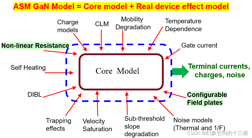
图2:ASM-HEMT核心和真实设备效果(由Khandelwal教授提供)
关于ASM-HEMT模型,已有详尽的文献。官方型号手册可以从这里下载。
关于模型方程的更多细节和背景,以下是出版时已知的文章列表。
ASM-HEMT参考文献
[1] U. K. Mishra, L. Shen, T. E. Kazior and Y.-F. Wu, “GaN-based RF power devices and amplifiers,” in IEEE, vol. 96, no. 2, February 2008, pp. 287{305.
[2] S. Khandelwal, “Compact modeling solutions for advanced semiconductor devices,” Ph.D. dissertation, Norwegian University of Science and Technology, 2013.
[3] S. Khandelwal, Y.S.Chauhan, and T.A.Fjeldly, “Analytical Modeling of Surface-Potential and Intrinsic Charges in AlGaN/GaN HEMT Devices,” IEEE Transactions on Electron Devices, vol. 59, no. 8, October 2012.
[4] S. Khandelwal, C. Yadav, S. Agnihotri, Y. S. Chauhan, A. Curutchet, T. Zimmer, J.-C. Dejaeger, N. Defrance, and T. A. Fjeldly, “A Robust Surface-Potential-Based Compact Model for GaN HEMT IC Design,” IEEE Transactions on Electron Devices, vol. 60, no. 10, October 2013.
[5] S. Ghosh, K. Sharma, S. Khandelwal, S. Agnihotri, T. A. Fjeldly, F. M. Yigletu, B. Iniguez, and Y. S. Chauhan, “Modeling of Temperature Effects in a Surface- Potential Based ASM-HEMT model,” in IEEE International Conference on Emerging Electronics (ICEE), Bangalore, 2014.
[6] S. Khandelwal, S. Ghosh, Y. S. Chauhan, B. Iniguez, T. A. Fjeldly and C. Hu, “Surface-Potential-Based RF Large-Signal Model for Gallium Nitride HEMTs,” in IEEE Compound Semiconductor IC Symposium (CSICS), New Orleans, USA, October 2015.
[7] S. A. Ahsan, S. Ghosh, K. Sharma, A. Dasgupta, S. Khandelwal, and Y. S. Chauhan, “Capacitance Modeling of a GaN HEMT with Gate and Source Field
Plates,” in IEEE International Symposium on Compound Semiconductors (ISCS), Santa Barbara, USA, June 2015.
[8] A. Dasgupta and Y. S. Chauhan, “Surface Potential Based Modeling of Induced Gate Thermal Noise for HEMTs,” in IEEE International Symposium on Compound Semiconductors (ISCS), Santa Barbara, USA, June 2015.
[9] S. Khandelwal, Y. S. Chauhan, B. Iniguez, and T. Fjeldly, “RF Large Signal Modeling of Gallium Nitride HEMTs with Surface-Potential Based ASM-HEMT Model,” in IEEE International Symposium on Compound Semiconductors (ISCS), Santa Barbara, USA, June 2015.
[10] A. Dasgupta, S. Ghosh, S. Khandelwal, and Y. S. Chauhan, “ASM-HEMT: Compact model for GaN HEMTs,” in IEEE Conference on Electron Devices and Solid-State Circuits (EDSSC), Singapore, June 2015.
[11] S. Ghosh, A. Dasgupta, S. Khandelwal, S. Agnihotri, and Y. S. Chauhan, “Surface-Potential-Based Compact Modeling of Gate Current in AlGaN/GaN HEMTs,” IEEE Transactions on Electron Devices, vol. 62, no. 2, February 2015.
[12] A. Dasgupta, S. Khandelwal, and Y. S. Chauhan, “Compact Modeling of Flicker Noise in HEMTs,” IEEE Journal of Electron Devices Society, vol. 2, no. 6, November 2014.
[13] A. Dasgupta, S. Khandelwal, and Y. S. Chauhan, “Surface potential based Modeling of Thermal Noise for HEMT circuit simulation,” IEEE Microwave and Wireless Components Letters, vol. 25, no. 6, June 2015.
[14] D.Delagebeaudeuf and N.T.Linh, “Metal-(n)AlGaAs-GaAs two-dimensional electron gas FET,” IEEE Transactions on Electron Devices, vol. 29, no. 1, pp. 955{960,1982.
[15] S. Kola, J. M. Golio, and G. N. Maracas, “An analytical expression for Fermi level versus sheet carrier concentration for HEMT modeling,” IEEE Transactions on Electron Devices, vol. 9, no. 2, pp. 136{138, 1988.
[16] F. M. Yigletu, B. Iniguez, S. Khandelwal, and T. A. Fjeldly, “A compact charge-based physical model for AlGaN/GaN HEMTs,” in Proc. Silicon Monolithic Integrated Circuits in RF Systems. Texas, USA, 2013, pp. 174-176.
[17] S. Khandelwal and T. A. Fjeldly, “A physics-based compact model of I-V and C-V characteristics in AlGaN/GaN HEMT devices,” Solid State Electronics, vol. 76, pp. 60-66, May 2012.
[18] S. Khandelwal, N. Goyal, and T. A. Fjeldly, “A precise physics-based compact model for 2-DEG charge density in AlGaAs/GaAs HEMTs applicable in all regions of device operation,” Solid State Electronics, vol. 79, pp. 22-25, 2013.
[19] S.Khandelwal, N. Goyal, and T. A. Fjeldly, “A Physics-based analytical model for 2-DEG charge density in AlGaN/GaN HEMT devices,” IEEE Transactions on Electron Devices, vol. 58, no. 10, pp. 3622-3625, October 2011.
[20] A. S. Householder, The Numerical Treatment of a Single Non-Linear Equation. McGraw Hill, 1970.
[21] S. Khandelwal and Tor A. Fjeldly, “Compact modeling of intrinsic capacitances in AlGaN/GaN HEMT devices,” in NSTI Nanotech, Boston, USA, vol. 2, June 2012, pp. 744-747.
[22] D. E. Ward, “Charge-based modeling of capacitance in MOS transistors,” Ph.D. dissertation, Stanford Univ., CA., 1981.
[23] S. Khandelwal, F. M. Yigletu, B. Iniguez, and T. A. Fjeldly, “A charge-based capacitance model for AlGaAs/GaAs HEMTs,” Solid State Electronics, vol. 82, pp. 38-40, January 2013.
[24] F. M. Yigletu, B. Iniguez, S. Khandelwal, and T. A. Fjeldly, “Compact physical models for gate charge and gate capacitance in AlGan/GaN HEMTs,” in Pros. of Simulation of Semiconductor Processes and Devices. Glasgow, UK, 2013.
[25] X. Cheng and Y.Wang, “A surface-potential-based compact model for AlGaN/GaN MODFETs,” IEEE Transactions on Electron Devices, vol. 58, no. 2, pp. 448-454, February 2011.
[26] S. Khandelwal, F. M. Yigletu, B. Iniguez, Tor A. Fjeldly, “Analytical modeling of surface-potential and drain current in AlGaAs/GaAs HEMTs,” in RF Integration Technology, Singapore, November 2012, pp. 183-185.
[27] S. Khandelwal, and Tor A. Fjeldly, “Analysis of Drain-Current Nonlinearity Using Surface-Potential-Based Model in GaAs pHEMTs,” IEEE Transactions on Microwave Theory and Techniques, vol. 61, no. 9, pp. 3265-3270, September 2013.
[28] S. Khandelwal, Nitin Goyal, and Tor A. Fjeldly, “Device geometry scalable thermal resistance model for GaN HEMT devices on Sapphire substrate,” in Reliability of Compound Semiconductor Workshop. Palm Springs, USA, April 2011.
[29] S. Khandelwal and Tor A. Fjeldly, “A surface-potential-based compact model for the study of non-linearities in AlGaAs/GaAs HEMTs,” in Compound Semiconductor IC Symposium (CSICS), San Diego, USA, October 2012, pp. 1{4.
[30] F. Mulugeta Yigletu, S. Khandelwal, T. A. Fjeldly, and B. Iniguez, “Compact charge-based physical models for current and capacitances in AlGaN/GaN HEMTs,” IEEE Transactions on Electron Devices, vol. 60, no. 11, pp. 3746-3752, November 2013.
ASM-HEMT 101.2参数表
以下参数是在ASM-HEMT 101.2手册1中发布的,并作为方便起见提供如下。
有关模型实现的详细信息,请参考该手册和Verilog-A代码。
- “AMSHEMT_1011.2.0技术手册”,Sourabh Khandelwal,Jason Hodges和Nikhil Reddy,澳大利亚悉尼麦考瑞大学。
实例参数
| 名称 | 单位 | 默认值 | 最小值 | 最大值 | 描述 |
|---|---|---|---|---|---|
| L | m | 0.25e-6 | 20e-9 | ∞ | 设计的栅极长度 |
| W | m | 200e-6 | 20e-9 | ∞ | 设计的栅极宽度 |
| NF | - | 1 | 1 | ∞ | 栅极指数 |
| SHMOD | - | 1 | 0 | 1 | 自热模型控制器,0-关闭自热模型 1-打开自热模型 |
| DFPL | m | 1e-6 | 0 | ∞ | 漏极-栅极接入区域长度 |
| NGCON | - | 1 | 1 | 2 | 栅极接触数 |
| DTEMP | 0 | -∞ | ∞ | 温度可变参数 |
处理参数
| 名称 | 单位 | 默认值 | 最小值 | 最大值 | 描述 |
|---|---|---|---|---|---|
| TNOM | °C | 27 | - | - | 常规温度 |
| TBAR | m | 2.5e-8 | 0.1e-9 | ∞ | AlGaN 层厚度 |
| L | m | 0.25e-6 | 20e-9 | ∞ | 设计栅极长度 |
| W | m | 200e-6 | 20e-9 | ∞ | 设计栅极宽度 |
| NF | - | 1 | 1 | ∞ | 栅极指数 |
| LSG | m | 1e-6 | 0 | ∞ | 源-栅极接入区长度 |
| LDG | m | 1e-6 | 0 | ∞ | 漏-栅极接入区长度 |
| EPSILON | F/m | 10.66e-11 | 0 | ∞ | AlGaN 层介电常数 |
| GAMMA0I | - | 2.120e-12 | 0 | 1 | 量子力学-泊松求解变量 |
| GAMMA1I | - | 3.73e-12 | 0 | 1 | 量子力学-泊松求解变量 |
IC-CAP软件学习交流群:941219939,欢迎进群学习讨论


 1248
1248

 被折叠的 条评论
为什么被折叠?
被折叠的 条评论
为什么被折叠?
 到【灌水乐园】发言


