


绪论
在一些应用中,两个电路模块交界处,一个电路模块的输出数据位宽大于另一个模块的输入数据位宽,此时需要进行数据转换。例如,在SATA控制器中,内部数据位宽为32比特,但是与外部物理收发器PHY的接口通常为16比特或8比特。同样的,从PHY接收到的数据也是16比特或8比特,数据交给控制器后,在其内部使用之前转换为32比特。下面将介绍进行数据宽度转换的电路,电路中没有使用FIFO,是通过时钟分频与倍频实现数据位宽转换和传输的。
由宽到窄数据转换
图6.30是位宽由宽变窄时的示意图。6.31是数据转换波形示意图。
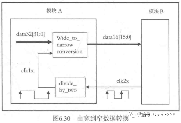
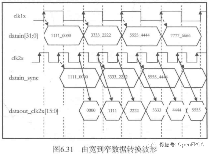
电路模块B的工作时钟为clk2x,在电路模块A中将其二分频得到clklX。clk1x与clk2x之间有一个同定的相位 差。根据图6.30和图6.31,具体的数据传输过程如下:
-
clklx下方的数据datain[31:0]经过clk2x采样产生datain_sync[31:0],由于clk1x在相位上滞后于clk2x且二者为同步时钟,因此数据从时钟域clklx传递到时钟域clk2x时不会存在问题;
-
在clk2x时钟域内,当clklx为0时,使用clk2x选择datain_sync的低16比特,当clklx为1时,选择datain_sync的高16比特;
-
完成数据变换,最终输出dataout_clk2x[15:0]。
代码及仿真结果如下。
module wide_to_narrow
(clk2x,
clklx,
datain,
dataout_clk2x);

input   clk2x;
input   clklx;
input [31: 0]   datain;
output [15: 0]   dataout_clk2x;
//***************************************

reg [31:0]    datain_sync;
reg [15:0]  dataout_clk2x;
wire [15:0]  dataout_clk2x_nxt;

// Flop the data first with clk2x. Reset is not required as it is a datapath and
// default (reset) value of the flops are don’t care.
//***************************************

always @(posedge clk2x)
begin
 datain_sync <- datain;
end

// Select the lower and upper halves from datain_sync
//***************************************

assign dataout_clk2x_nxt = !clk 1 x ? datain_sync[15:0] :datain_sync[31:16];

// Flop the selected 16 bit data with clk2x and drive out
//***************************************

always @(posedge clk2x)
begin
 dataout_clk2x <= dataout_clk2x_nxt;
end

endmodule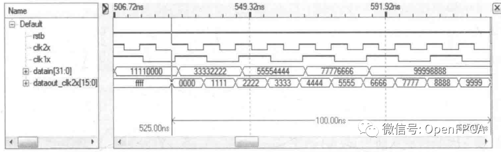
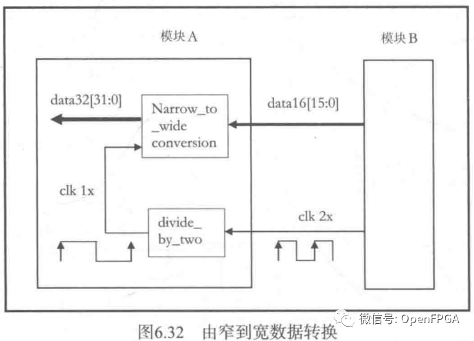
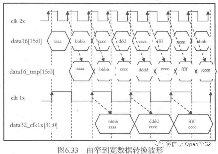
由窄到宽数据转换
图6.32和图6.33是实现由窄到宽数据转换操作的电路和工作波形。
代码及仿真结果如下。
module narrow_to_wide
(clk2x,
clklx,
data16,
data32_clk1x);

input   clk2x;
input   clklx;
input [15: 0]   data16;
output [31: 0]   data32_clk1x;
//***************************************

reg [15:0]    data16_tmp;
reg [31:0]  data32_clk1x data32_clk1x_nxt;

/* store temporary data into a register
along with the 16 bits of tmp data stored in pervious cycle to form 32 bits of data.
These 32 bits of data is flopped with clklx, and this happens for every two-clock
periods of clk2x.

When data is passed from 2x (fast) to the lx (slow) domain, make sure that there is
enough delay in the data path to avoid set-up/hold violation in the immediate risi
edge of lx clock. The data should have more delay in the path to pass beyond
immediate rising edge of 1x clock*/

//***************************************

always @(posedge clk2x)
begin
 datal6_tmp <= #2 datal 6;
end
// Form the 32-bit data
 assign data32_clklx_nxt = {datal 6[15:0], data16_tmp[l5:0]};
// Flop the selected 16 bit data with clk2x and drive out
always @(posedge elklx)
begin
 data32_clklx <= data32_clklx_nxt;
end
endmodule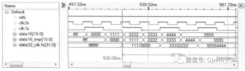

NOW现在行动!

学习Xilinx FPGA最好的资料其实就是官方手册,下表总结了部分手册的主要介绍内容,关注我,持续更新中......
| 文件名 | 主标题 | 内容简单介绍 | 是否有中文版 | |
| UG476 | 7 Series FPGAs GTX/GTH Transceivers | GTX和GTH介绍,PCIe、serdes等学习必备 | 否 | |
| UG471 | 7 Series FPGAs SelectIO Resources | 描述 7 系列 FPGA 中可用的 SelectIO资源。 | 否 | |
| UG1114 | PetaLinux Tools Documentaton | PetaLinux 工具文档 参考指南 | 是,V2019.2 | |
| UG949 | UltraFAST 设计方法指南(适用于 Vivado Design Suite) | 赛灵思® UltraFast™ 设计方法是用于为当今器件优化设计进程的一套最佳实践。这些设计的规模与复杂性需要执行特定的步骤与设计任务,从而确保设计每一个阶段的成功开展。依照这些步骤,并遵循最佳实践,将帮助您以最快的速度和最高的效率实现期望的设计目标 | 是,V2018.1 | |
| IP手册 | pg057 | FIFO Generator | FIFO生成器IP使用手册 | 否 |
| pg104 | Complex Multiplier | 复数乘法器IP使用手册 | 否 | |
| pg122 | RAM-Based Shift Register | 移位寄存器IP使用手册 | 否 |

推荐阅读
【Vivado那些事】Vivado中常用的快捷键(二)其他常用快捷键
图书推荐|ARM Cortex-M0 全可编程SoC原理及实现
1202年了,还在使用虚拟机吗?Win10安装Ubuntu子系统及图形化界面详细教程
Github 上有哪些优秀的 VHDL/Verilog/FPGA 项目
高速串行通信常用的编码方式-8b/10b编码/解码
Verilog计时(微秒、毫秒和秒)脉冲的产生及同步整形电路
再说System Verilog 与 Verilog 的关系


 1562
1562


 被折叠的 条评论
为什么被折叠?
被折叠的 条评论
为什么被折叠?
 到【灌水乐园】发言


